SBOSA58 February 2021 OPA858-Q1
PRODUCTION DATA
- 1 Features
- 2 Applications
- 3 Description
- 4 Revision History
- 5 Pin Configuration and Functions
- 6 Specifications
- 7 Parameter Measurement Information
- 8 Detailed Description
- 9 Application and Implementation
- 10Power Supply Recommendations
- 11Layout
- 12Device and Documentation Support
- 13Mechanical, Packaging, and Orderable Information
Package Options
Mechanical Data (Package|Pins)
- DSG|8
Thermal pad, mechanical data (Package|Pins)
- DSG|8
Orderable Information
3 Description
The OPA858-Q1 is a wideband, low-noise operational amplifier with CMOS inputs for wideband transimpedance and voltage amplifier applications. When the device is configured as a transimpedance amplifier (TIA), the 5.5-GHz gain bandwidth product (GBWP) enables high closed-loop bandwidths at transimpedance gains in the range of tens to hundreds of kΩs.
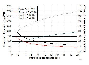
The graph below shows the bandwidth and noise performance of the OPA858-Q1 as a function of the photodiode capacitance when the amplifier is configured as a TIA. The total noise is calculated along a bandwidth range extending from DC to the calculated frequency (f) on the left scale. The OPA858-Q1 package has a feedback pin (FB) that simplifies the feedback network connection between the input and the output.
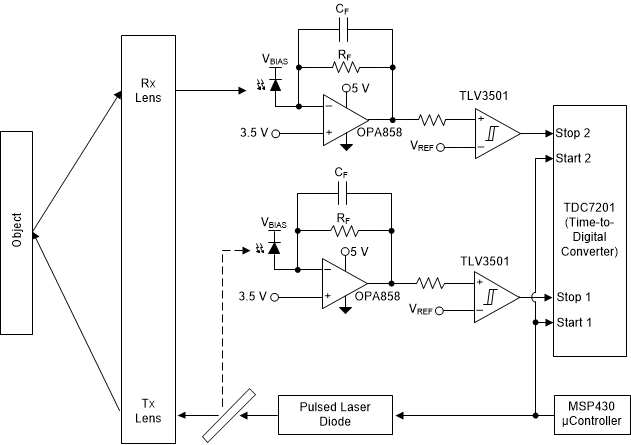
The OPA858-Q1 is optimized to operate in optical time-of-flight (ToF) systems where the OPA858-Q1 is used with time-to-digital converters, such as the TDC7201. Use the OPA858-Q1 to drive a high-speed analog-to-digital converter (ADC) in high-resolution LIDAR systems with a differential output amplifier, such as the THS4541-Q1.
| PART NUMBER(1) | PACKAGE | BODY SIZE (NOM) |
|---|---|---|
| OPA858-Q1 | WSON (8) | 2.00 mm × 2.00 mm |
 High-Speed
Time-of-Flight Receiver
 Photodiode
Capacitance vs Bandwidth and Noise