SBOSA58 February 2021 OPA858-Q1
PRODUCTION DATA
- 1 Features
- 2 Applications
- 3 Description
- 4 Revision History
- 5 Pin Configuration and Functions
- 6 Specifications
- 7 Parameter Measurement Information
- 8 Detailed Description
- 9 Application and Implementation
- 10Power Supply Recommendations
- 11Layout
- 12Device and Documentation Support
- 13Mechanical, Packaging, and Orderable Information
Package Options
Mechanical Data (Package|Pins)
- DSG|8
Thermal pad, mechanical data (Package|Pins)
- DSG|8
Orderable Information
9.2.2 Detailed Design Procedure
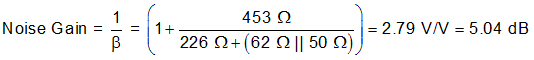
The OPA858-Q1 is compensated to have less than 1 dB of peaking in a gain of 7 V/V. Using the device in lower gains results in increased peaking and potential instability. Figure 9-4 shows the OPA858-Q1 configured in a signal gain of –2 V/V. The DC noise gain (1/β) of the amplifier is affected by the 62-Ω termination resistor and the 50-Ω source resistor and is given by Equation 1. At higher frequencies the noise gain is affected by reactive elements such as inductors and capacitors. These include both discrete board components as well as printed circuit board (PCB) parasitics.
The stability and phase margin of the amplifier depend on the loop gain of the amplifier, which is the product of the AOL and the feedback factor (β) of the amplifier. The β of a negative-feedback loop system is the portion of the output signal that is fed back to the input, and in the case of an amplifier is the inverse of the noise gain. The noise gain of the amplifier at high frequencies can be increased by adding an input capacitor and a feedback capacitor as Figure 9-5 shows. If done carefully, increasing 1/β improves the phase margin just as any amplifier is more stable in a high gain configuration versus a unity-gain buffer configuration. The modified network with the added capacitors alters the high-frequency noise gain, but does not alter the signal gain. The AN-1604 Decompensated Operational Amplifiers application report provides a detailed analysis of noise gain-shaping techniques for decompensated amplifiers and shows how to choose external resistors and capacitor values.
Figure 9-6 shows the uncompensated frequency response of the OPA858-Q1 configured as shown in Figure 9-4. Without any added noise gain shaping components, the OPA858-Q1 shows approximately 13 dB of peaking.
Figure 9-7 shows the noise gain compensated frequency response of the OPA858-Q1 configured as shown in Figure 9-5. The noise gain shaping elements reduce the peaking to less than 1.5 dB. The 2.7-pF input capacitor, the input capacitance of the amplifier, the gain resistor, and the feedback resistor create a zero in the noise gain at a frequency f, as Equation 2 shows.
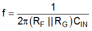
where
- RF is the feedback resistor
- RG is the input or gain resistor (includes the effect of the source and termination resistor)
- CIN is the total input capacitance, which includes the external 2.7-pF capacitor, the amplifier input capacitance, and any parasitic PCB capacitance.
The zero in Equation 2 increases the noise gain at higher frequencies, which is important when compensating a decompensated amplifier. However, the noise gain zero reduces the loop gain phase which results in a lower phase margin. To counteract the phase reduction due to the noise gain zero, add a pole to the noise gain curve by inserting the 0.5-pF feedback capacitor. The pole occurs at a frequency shown in Equation 3. The noise gain pole and zero locations must be selected so that the rate-of-closure between the magnitude curves of AOL and 1/β is approximately 20 dB. To ensure this, the noise gain pole must occur before the 1/β magnitude curve intersects the AOL magnitude curve. In other words, the noise gain pole must occur before |AOL| = |1/β|. The point at which the two curves intersect is known as the loop gain crossover frequency.
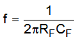
where
- CF is the feedback capacitor (includes any added PCB parasitic)
For more information on op amp stability, watch the TI Precision Lab series on stability video.