SCPS143G June 2009 – March 2021 PCA9548A
PRODUCTION DATA
- 1 Features
- 2 Applications
- 3 Description
- 4 Revision History
- 5 Pin Configuration and Functions
- 6 Specifications
- 7 Parameter Measurement Information
- 8 Detailed Description
- 9 Application Information Disclaimer
- 10Power Supply Recommendations
- 11Layout
- 12Device and Documentation Support
- 13Mechanical, Packaging, and Orderable Information
Package Options
Mechanical Data (Package|Pins)
Thermal pad, mechanical data (Package|Pins)
- RGE|24
Orderable Information
8.6.2 Control Register
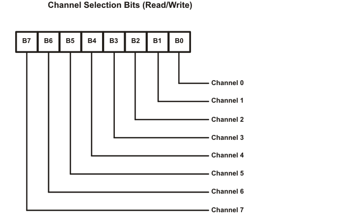
Following the successful acknowledgment of the address byte, the bus master sends a command byte that is stored in the control register in the PCA9548A (see Figure 8-5). This register can be written and read via the I2C bus. Each bit in the command byte corresponds to a SCn/SDn channel and a high (or 1) selects this channel. Multiple SCn/SDn channels may be selected at the same time. When a channel is selected, the channel becomes active after a stop condition has been placed on the I2C bus. This ensures that all SCn/SDn lines are in a high state when the channel is made active, so that no false conditions are generated at the time of connection. A stop condition always must occur immediately after the acknowledge cycle. If multiple bytes are received by the PCA9548A, it saves the last byte received.
 Figure 8-5 Control Register
Table 8-2 shows the PCA9548A Command byte definition.
| CONTROL REGISTER BITS | COMMAND | |||||||
|---|---|---|---|---|---|---|---|---|
| B7 | B6 | B5 | B4 | B3 | B2 | B1 | B0 | |
| X | X | X | X | X | X | X | 0 | Channel 0 disabled |
| 1 | Channel 0 enabled | |||||||
| X | X | X | X | X | X | 0 | X | Channel 1 disabled |
| 1 | Channel 1 enabled | |||||||
| X | X | X | X | X | 0 | X | X | Channel 2 disabled |
| 1 | Channel 2 enabled | |||||||
| X | X | X | X | 0 | X | X | X | Channel 3 disabled |
| 1 | Channel 3 enabled | |||||||
| X | X | X | 0 | X | X | X | X | Channel 4 disabled |
| 1 | Channel 4 enabled | |||||||
| X | X | 0 | X | X | X | X | X | Channel 5 disabled |
| 1 | Channel 5 enabled | |||||||
| X | 0 | X | X | X | X | X | X | Channel 6 disabled |
| 1 | Channel 6 enabled | |||||||
| 0 | X | X | X | X | X | X | X | Channel 7 disabled |
| 1 | Channel 7 enabled | |||||||
| 0 | 0 | 0 | 0 | 0 | 0 | 0 | 0 | No channel selected, power-up/reset default state |