SCPS143G June   2009  – March 2021 PCA9548A

PRODUCTION DATA  

  1. Features
  2. Applications
  3. Description
  4. Revision History
  5. Pin Configuration and Functions
  6. Specifications
    1. 6.1 Absolute Maximum Ratings
    2. 6.2 ESD Ratings
    3. 6.3 Recommended Operating Conditions
    4. 6.4 Thermal Information
    5. 6.5 Electrical Characteristics
    6. 6.6 I2C Interface Timing Requirements
    7. 6.7 Reset Timing Requirements
    8. 6.8 Switching Characteristics
    9. 6.9 Typical Characteristics
  7. Parameter Measurement Information
  8. Detailed Description
    1. 8.1 Overview
    2. 8.2 Functional Block Diagram
    3. 8.3 Feature Description
    4. 8.4 Device Functional Modes
      1. 8.4.1 RESET Input
        1. 8.4.1.1 RESET Errata
          1. 8.4.1.1.1 System Impact
          2. 8.4.1.1.2 System Workaround
      2. 8.4.2 Power-On Reset
    5. 8.5 Programming
      1. 8.5.1 I2C Interface
    6. 8.6 Register Maps
      1. 8.6.1 Device Address
      2. 8.6.2 Control Register
      3. 8.6.3 Bus Transactions
        1. 8.6.3.1 Writes
        2. 8.6.3.2 Reads
  9. Application Information Disclaimer
    1. 9.1 Application Information
    2. 9.2 Typical Application
      1. 9.2.1 Design Requirements
      2. 9.2.2 Detailed Design Procedure
      3. 9.2.3 Application Curves
  10. 10Power Supply Recommendations
    1. 10.1 Power-On Reset Requirements
  11. 11Layout
    1. 11.1 Layout Guidelines
    2. 11.2 Layout Example
  12. 12Device and Documentation Support
    1. 12.1 Related Documentation
    2. 12.2 Receiving Notification of Documentation Updates
    3. 12.3 Support Resources
    4. 12.4 Trademarks
    5. 12.5 Electrostatic Discharge Caution
    6. 12.6 Glossary
  13. 13Mechanical, Packaging, and Orderable Information

Package Options

Mechanical Data (Package|Pins)
Thermal pad, mechanical data (Package|Pins)
Orderable Information

Typical Application

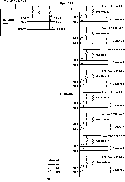
A typical application of the PCA9548A contains 1 or many separate data pull-up voltages, VCC , one for the master device and one for each of the selectable slave channels, 0 through 7. In the event where the master device and all slave devices operate at the same voltage, then the VCC pin can be connected to this supply voltage. In an application where voltage translation is necessary, additional design requirements must be considered (See the Design Requirements section).

Figure 9-1 shows an application in which the PCA9548A can be used.
GUID-FC8633EC-0D71-4DBA-A201-7260A3777F6B-low.gif
Pin numbers shown are for the PW and RTW packages.
Figure 9-1 PCA9548A Typical Application Schematic