SCPS131J August 2005 – March 2021 PCA9555
PRODUCTION DATA
- 1 Features
- 2 Applications
- 3 Description
- 4 Revision History
- 5 Pin Configuration and Functions
- 6 Specifications
- 7 Parameter Measurement Information
- 8 Detailed Description
- 9 Application Information Disclaimer
- 10Power Supply Recommendations
- 11Layout
- 12Device and Documentation Support
- 13Mechanical, Packaging, and Orderable Information
Package Options
Mechanical Data (Package|Pins)
Thermal pad, mechanical data (Package|Pins)
- RGE|24
Orderable Information
8.5.2.4.1 Writes
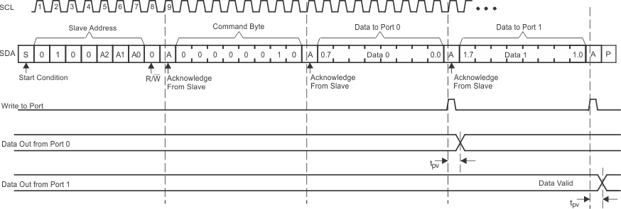
Data is transmitted to the PCA9555 by sending the device address and setting the least-significant bit to a logic 0 (see Figure 8-6 for device address). The command byte is sent after the address and determines which register receives the data that follows the command byte.
The eight registers within the PCA9555 are configured to operate as four register pairs. The four pairs are input ports, output ports, polarity inversion ports, and configuration ports. After sending data to one register, the next data byte is sent to the other register in the pair (see Figure 8-8 and Figure 8-9). For example, if the first byte is sent to output port (register 3), the next byte is stored in Output Port 0 (register 2).
There is no limitation on the number of data bytes sent in one write transmission. In this way, each 8-bit register may be updated independently of the other registers.
 Figure 8-8 Write To Output Port Registers
 Figure 8-9 Write To Configuration Registers