SCPS068J July 2001 – March 2015 PCF8574
PRODUCTION DATA.
- 1 Features
- 2 Applications
- 3 Description
- 4 Revision History
- 5 Pin Configuration and Functions
- 6 Specifications
- 7 Parameter Measurement Information
- 8 Detailed Description
- 9 Application and Implementation
- 10Power Supply Recommendations
- 11Layout
- 12Device and Documentation Support
- 13Mechanical, Packaging, and Orderable Information
11 Layout
11.1 Layout Guidelines
For printed circuit board (PCB) layout of the PCF8574 device, common PCB layout practices should be followed but additional concerns related to high-speed data transfer such as matched impedances and differential pairs are not a concern for I2C signal speeds.
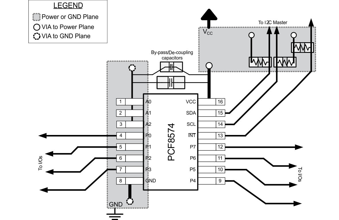
In all PCB layouts, it is a best practice to avoid right angles in signal traces, to fan out signal traces away from each other upon leaving the vicinity of an integrated circuit (IC), and to use thicker trace widths to carry higher amounts of current that commonly pass through power and ground traces. By-pass and de-coupling capacitors are commonly used to control the voltage on the VCC pin, using a larger capacitor to provide additional power in the event of a short power supply glitch and a smaller capacitor to filter out high-frequency ripple. These capacitors should be placed as close to the PCF8574 device as possible. These best practices are shown in Figure 27.
For the layout example provided in Figure 27, it would be possible to fabricate a PCB with only 2 layers by using the top layer for signal routing and the bottom layer as a split plane for power (VCC) and ground (GND). However, a 4 layer board is preferable for boards with higher density signal routing. On a 4 layer PCB, it is common to route signals on the top and bottom layer, dedicate one internal layer to a ground plane, and dedicate the other internal layer to a power plane. In a board layout using planes or split planes for power and ground, vias are placed directly next to the surface mount component pad which needs to attach to VCC or GND and the via is connected electrically to the internal layer or the other side of the board. Vias are also used when a signal trace needs to be routed to the opposite side of the board, but this technique is not demonstrated in Figure 27.
11.2 Layout Example
 Figure 27. Layout Example for PCF8574