SCPS121H January   2005  – February 2020 PCF8575

PRODUCTION DATA.  

  1. Features
  2. Applications
  3. Description
    1.     Device Images
      1.      Simplified Schematic
  4. Revision History
  5. Pin Configuration and Functions
    1.     Pin Functions
  6. Specifications
    1. 6.1 Absolute Maximum Ratings
    2. 6.2 ESD Ratings
    3. 6.3 Recommended Operating Conditions
    4. 6.4 Thermal Information
    5. 6.5 Electrical Characteristics
    6. 6.6 I2C Interface Timing Requirements
    7. 6.7 Switching Characteristics
    8. 6.8 Typical Characteristics
  7. Parameter Measurement Information
  8. Detailed Description
    1. 8.1 Overview
    2. 8.2 Functional Block Diagram
      1. 8.2.1 Logic Diagram (Positive Logic)
      2. 8.2.2 Simplified Schematic Diagram of Each P-Port Input/Output
    3. 8.3 Feature Description
      1. 8.3.1 I2C Interface
      2. 8.3.2 Interface Definition
      3. 8.3.3 Address Reference
    4. 8.4 Device Functional Modes
  9. Application and Implementation
    1. 9.1 Application Information
    2. 9.2 Typical Application
      1. 9.2.1 Design Requirements
        1. 9.2.1.1 Minimizing ICC When I/Os Control LEDs
      2. 9.2.2 Detailed Design Procedure
      3. 9.2.3 Application Curves
  10. 10Power Supply Recommendations
    1. 10.1 Power-On Reset
    2. 10.2 System Impact
  11. 11Layout
    1. 11.1 Layout Guidelines
    2. 11.2 Layout Example
  12. 12Device and Documentation Support
    1. 12.1 Device Support
    2. 12.2 Documentation Support
    3. 12.3 Receiving Notification of Documentation Updates
    4. 12.4 Support Resources
    5. 12.5 Trademarks
    6. 12.6 Electrostatic Discharge Caution
    7. 12.7 Glossary
  13. 13Mechanical, Packaging, and Orderable Information

Package Options

Mechanical Data (Package|Pins)
Thermal pad, mechanical data (Package|Pins)
Orderable Information

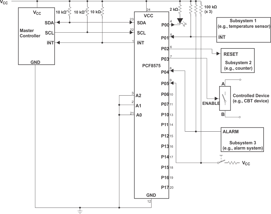
Typical Application

PCF8575 typ_app_cps121.gif
The SCL and SDA pins must be tied directly to VCC because if SCL and SDA are tied to an auxiliary power supply that could be powered on while VCC is powered off, then the supply current, ICC, will increase as a result.
Device address is configured as 0100000 for this example.
P0, P2, and P3 are configured as outputs.
P1, P4, and P5 are configured as inputs.
P6 and P7 are not used and must be configured as outputs.
Figure 20. Application Schematic