SLES211C February 2008 – July 2015 PCM1681 , PCM1681-Q1
PRODUCTION DATA.
- 1 Features
- 2 Applications
- 3 Description
- 4 Revision History
- 5 Description (continued)
- 6 Pin Configuration and Functions
- 7 Specifications
-
8 Detailed Description
- 8.1 Overview
- 8.2 Functional Block Diagram
- 8.3 Feature Description
- 8.4 Device Functional Modes
- 8.5 Programming
- 8.6
Register Maps
- 8.6.1 Reserved Registers
- 8.6.2
Register Definitions
- 8.6.2.1 ATx[7:0]: Digital Attenuation Level Setting
- 8.6.2.2 MUTx: Soft Mute Control
- 8.6.2.3 DACx: DAC Operation Control
- 8.6.2.4 FLT: Digital Filter Roll-Off Control
- 8.6.2.5 FMT[3:0]: Audio Interface Data Format
- 8.6.2.6 SRST: Reset
- 8.6.2.7 ZREV: Zero-Flag Polarity Select
- 8.6.2.8 DREV: Output Phase Select
- 8.6.2.9 DMF[1:0]: Sampling Frequency Selection for the De-Emphasis Function
- 8.6.2.10 DMC: Digital De-Emphasis All-Channel Function Control
- 8.6.2.11 REV[8:1]: Output Phase Select per Channel
- 8.6.2.12 OVER: Oversampling Rate Control
- 8.6.2.13 FLTx: Digital Filter Roll-Off Control per DATA Group
- 8.6.2.14 DAMS: Digital Attenuation Mode Select
- 8.6.2.15 AZRO[1:0]: Zero-Flag Channel-Combination Select
- 8.6.2.16 ZERO[8:1]: Zero-Detect Status (Read-Only, I2C Interface Only)
- 9 Application and Implementation
- 10Power Supply Recommendations
- 11Layout
- 12Device and Documentation Support
- 13Mechanical, Packaging, and Orderable Information
Package Options
Mechanical Data (Package|Pins)
- PWP|28
Thermal pad, mechanical data (Package|Pins)
- PWP|28
Orderable Information
1 Features
- Qualified for Automotive Applications: PCM1681-Q1
- 24-Bit Resolution
- Analog Performance:
- Dynamic Range: 105 dB Typical
- SNR: 105 dB Typical
- THD+N: 0.002% Typical
- Full-Scale Output: 3.75 VPP Typical
- 4×/8× Oversampling Interpolation Filter:
- Stop-Band Attenuation: –57 dB
- Pass-Band Ripple: ±0.015 dB
- Sampling Frequency: 5 kHz to 200 kHz
- System Clock: 128 fS, 192 fS, 256 fS, 384 fS, 512 fS, 768 fS, or 1152 fS with Autodetect
- Zero Flags for Selectable Channel Combinations
- Flexible Mode Control:
- SPI™/I2C™ Dual Mode for Serial Port
- Parallel Hardware Control with 4 Functions
- User-Programmable Functions (in SPI/I2C):
- Flexible Audio Data Formats:
- Right-Justified, I2S™, Left-Justified, TDM, DSP
- 16- and 24-Bit Audio Data
- Digital Attenuation: Mode Selectable
- 0 dB to –63 dB, 0.5 dB/step
- 0 dB to –100 dB, 1 dB/step
- Soft Mute
- Digital De-Emphasis
- Digital Filter Roll-Off: Sharp or Slow
- Oversampling Mode
- Flexible Audio Data Formats:
- User-Programmable Functions (in H/W):
- Flexible Audio Data Formats:
- Right-Justified, I2S, Left-Justified, TDM
- Soft Mute
- Digital De-Emphasis
- Oversampling Mode
- Flexible Audio Data Formats:
- Power Supply Voltage: 5-V Analog, 3.3-V Digital
- Package: 28-Lead HTSSOP PowerPAD™
- Operation Temperature Range:
- –40°C to 85°C for Consumer Grade
- –40°C to 105°C for Automotive Audio Grade
2 Applications
3 Description
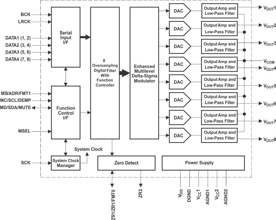
The PCM1681 and PCM1681-Q1 are CMOS monolithic integrated circuits which feature an eight-channel 24-bit audio digital-to-analog converter (DAC) and support circuitry in small 28-lead TSSOP PowerPAD packages. The DACs utilize Burr-Brown's enhanced multilevel delta-sigma (ΔΣ) architecture to achieve excellent signal-to-noise performance and a high tolerance to clock jitter.
Device Information(1)
| PART NUMBER | PACKAGE | BODY SIZE (NOM) |
|---|---|---|
| PCM1681 | HTSSOP (28) | 9.70 mm × 4.40 mm |
| PCM1681-Q1 |
- For all available packages, see the orderable addendum at the end of the datasheet.
Functional Block Diagram
