SBAS989 April 2019 PCM1840
PRODUCTION DATA.
- 1 Features
- 2 Applications
- 3 Description
- 4 Revision History
- 5 Pin Configuration and Functions
- 6 Specifications
-
7 Detailed Description
- 7.1 Overview
- 7.2 Functional Block Diagram
- 7.3
Feature Description
- 7.3.1 Hardware Control
- 7.3.2 Audio Serial Interfaces
- 7.3.3 Phase-Locked Loop (PLL) and Clock Generation
- 7.3.4 Input Channel Configurations
- 7.3.5 Reference Voltage
- 7.3.6 Microphone Bias
- 7.3.7
Signal-Chain Processing
- 7.3.7.1 Digital High-Pass Filter
- 7.3.7.2
Configurable Digital Decimation Filters
- 7.3.7.2.1
Linear Phase Filters
- 7.3.7.2.1.1 Sampling Rate: 8 kHz or 7.35 kHz
- 7.3.7.2.1.2 Sampling Rate: 16 kHz or 14.7 kHz
- 7.3.7.2.1.3 Sampling Rate: 24 kHz or 22.05 kHz
- 7.3.7.2.1.4 Sampling Rate: 32 kHz or 29.4 kHz
- 7.3.7.2.1.5 Sampling Rate: 48 kHz or 44.1 kHz
- 7.3.7.2.1.6 Sampling Rate: 96 kHz or 88.2 kHz
- 7.3.7.2.1.7 Sampling Rate: 192 kHz or 176.4 kHz
- 7.3.7.2.2 Low-Latency Filters
- 7.3.7.2.1
Linear Phase Filters
- 7.3.8 Dynamic Range Enhancer (DRE)
- 7.4 Device Functional Modes
- 8 Application and Implementation
- 9 Power Supply Recommendations
- 10Layout
- 11Device and Documentation Support
- 12Mechanical, Packaging, and Orderable Information
Package Options
Mechanical Data (Package|Pins)
- RTW|24
Thermal pad, mechanical data (Package|Pins)
- RTW|24
Orderable Information
7.3.7.2.1.7 Sampling Rate: 192 kHz or 176.4 kHz
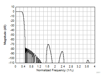
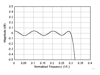
Figure 36 and Figure 37 respectively show the magnitude response and the pass-band ripple for a decimation filter with a sampling rate of 192 kHz or 176.4 kHz. Table 14 lists the specifications for a decimation filter with an 192-kHz or 176.4-kHz sampling rate.
 Figure 36. Linear Phase Decimation Filter Magnitude Response
  Figure 37. Linear Phase Decimation Filter Pass-Band Ripple
 Table 14. Linear Phase Decimation Filter Specifications
| PARAMETER | TEST CONDITIONS | MIN | TYP | MAX | UNIT |
|---|---|---|---|---|---|
| Pass-band ripple | Frequency range is 0 to 0.3 × fS | –0.05 | 0.05 | dB | |
| Stop-band attenuation | Frequency range is 0.473 × fS to 4 × fS | 70.0 | dB | ||
| Frequency range is 4 × fS onwards | 111.0 | ||||
| Group delay or latency | Frequency range is 0 to 0.3 × fS | 11.9 | 1/fS |