SBASA30 December 2020 PCM6480-Q1
PRODUCTION DATA
- 1 Features
- 2 Applications
- 3 Description
- 4 Revision History
- 5 Device Comparison Table
- 6 Pin Configuration and Functions
-
7 Specifications
- 7.1 Absolute Maximum Ratings
- 7.2 ESD Ratings
- 7.3 Recommended Operating Conditions
- 7.4 Thermal Information
- 7.5 Electrical Characteristics
- 7.6 Timing Requirements: I2C Interface
- 7.7 Switching Characteristics: I2C Interface
- 7.8 Timing Requirements: SPI Interface
- 7.9 Switching Characteristics: SPI Interface
- 7.10 Timing Requirements: TDM, I2S or LJ Interface
- 7.11 Switching Characteristics: TDM, I2S or LJ Interface
- 7.12 Timing Requirements: PDM Digital Microphone Interface
- 7.13 Switching Characteristics: PDM Digial Microphone Interface
- 7.14 Timing Diagrams
- 7.15 Typical Characteristics
-
8 Detailed Description
- 8.1 Overview
- 8.2 Functional Block Diagram
- 8.3
Feature Description
- 8.3.1 Serial Interfaces
- 8.3.2 Phase-Locked Loop (PLL) and Clock Generation
- 8.3.3 Analog Input Channel Configuration
- 8.3.4 Reference Voltage
- 8.3.5 Microphone Bias
- 8.3.6 Input DC Fault Diagnostics
- 8.3.7 Digital PDM Microphone Record Channel
- 8.3.8
Signal-Chain Processing
- 8.3.8.1 Programmable Channel Gain and Digital Volume Control
- 8.3.8.2 Programmable Channel Gain Calibration
- 8.3.8.3 Programmable Channel Phase Calibration
- 8.3.8.4 Programmable Digital High-Pass Filter
- 8.3.8.5 Programmable Digital Biquad Filters
- 8.3.8.6 Programmable Channel Summer and Digital Mixer
- 8.3.8.7
Configurable Digital Decimation Filters
- 8.3.8.7.1
Linear Phase Filters
- 8.3.8.7.1.1 Sampling Rate: 8 kHz or 7.35 kHz
- 8.3.8.7.1.2 Sampling Rate: 16 kHz or 14.7 kHz
- 8.3.8.7.1.3 Sampling Rate: 24 kHz or 22.05 kHz
- 8.3.8.7.1.4 Sampling Rate: 32 kHz or 29.4 kHz
- 8.3.8.7.1.5 Sampling Rate: 48 kHz or 44.1 kHz
- 8.3.8.7.1.6 Sampling Rate: 96 kHz or 88.2 kHz
- 8.3.8.7.1.7 Sampling Rate: 192 kHz or 176.4 kHz
- 8.3.8.7.1.8 Sampling Rate: 384 kHz or 352.8 kHz
- 8.3.8.7.1.9 Sampling Rate: 768 kHz or 705.6 kHz
- 8.3.8.7.2 Low-Latency Filters
- 8.3.8.7.3
Ultra-Low-Latency Filters
- 8.3.8.7.3.1 Sampling Rate: 16 kHz or 14.7 kHz
- 8.3.8.7.3.2 Sampling Rate: 24 kHz or 22.05 kHz
- 8.3.8.7.3.3 Sampling Rate: 32 kHz or 29.4 kHz
- 8.3.8.7.3.4 Sampling Rate: 48 kHz or 44.1 kHz
- 8.3.8.7.3.5 Sampling Rate: 96 kHz or 88.2 kHz
- 8.3.8.7.3.6 Sampling Rate: 192 kHz or 176.4 kHz
- 8.3.8.7.3.7 Sampling Rate: 384 kHz or 352.8 kHz
- 8.3.8.7.1
Linear Phase Filters
- 8.3.9 Automatic Gain Controller (AGC)
- 8.3.10 Interrupts, Status, and Digital I/O Pin Multiplexing
- 8.4 Device Functional Modes
- 8.5 Programming
- 8.6 Register Maps
- 9 Application and Implementation
- 10Power Supply Recommendations
- 11Layout
- 12Device and Documentation Support
- 13Mechanical, Packaging, and Orderable Information
Package Options
Mechanical Data (Package|Pins)
- RTV|32
Thermal pad, mechanical data (Package|Pins)
Orderable Information
8.3.8.6 Programmable Channel Summer and Digital Mixer
For applications that require an even higher SNR than that supported for each channel, the device digital summing mode can be used. In this mode, the digital record data are summed up across the channel with an equal weightage factor, which helps in reducing the effective record noise. Table 8-18 lists the configuration settings available for channel summing mode.
| P0_R107_D[3:2] : CH_SUM[2:0] | CHANNEL SUMMING MODE FOR INPUT CHANNELS | SNR AND DYNAMIC RANGE BOOST |
|---|---|---|
| 00 (Default) | Channel summing mode is disabled | Not applicable |
| 01 | Output channel 1 = (input channel 1 + input channel 2) / 2 | 3-dB boost in SNR and dynamic range |
| Output channel 2 = (input channel 1 + input channel 2) / 2 | ||
| Output channel 3 = (input channel 3 + input channel 4) / 2 | 3-dB boost in SNR and dynamic range | |
| Output channel 4 = (input channel 3 + input channel 4) / 2 | ||
| 10 | Output channel 1 = (input channel 1 + input channel 2 + input channel 3 + input channel 4) / 4 | 6-dB boost in SNR and dynamic range |
| Output channel 2 = (input channel 1 + input channel 2 + input channel 3 + input channel 4) / 4 | ||
| Output channel 3 = (input channel 1 + input channel 2 + input channel 3 + input channel 4) / 4 | ||
| Output channel 4 = (input channel 1 + input channel 2 + input channel 3 + input channel 4) / 4 | ||
| 11 | Reserved (do not use this setting) | Not applicable |
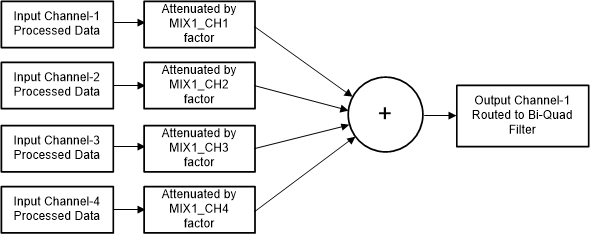
The device additionally supports a fully programmable mixer feature that can mix the various input channels with their custom programmable scale factor to generate the final output channels. The programmable mixer feature is available only if CH_SUM[2:0] is set to 2'b00. The mixer function is only supported for input channel 1 to channel 4. Figure 8-24 shows a block diagram that describes the mixer 1 operation to generate output channel 1. The programmable coefficients for the mixer operation are located in the Section 8.6.2.3 section. All mixer coefficients are 32-bit, two’s complement numbers using a 1.31 number format. The value of 0x7FFFFFFF is equivalent to +1 (0-dB gain), the value 0x00000000 is equivalent to mute (zero data), and any values in between set the mixer attenuation computed using Equation 3. If the MSB is set to '1' then the attenuation remains the same but the signal phase is inverted.
 Figure 8-24 Programmable Digital Mixer Block Diagram
A similar mixer operation is performed by mixer 2, mixer 3, and mixer 4 to generate output channel 2, channel 3, and channel 4, respectively.