SBOS487B June 2009 – March 2020 PGA280
PRODUCTION DATA.
- 1 Features
- 2 Applications
- 3 Description
- 4 Revision History
- 5 Pin Configuration and Functions
- 6 Specifications
-
7 Detailed Description
- 7.1 Overview
- 7.2 Functional Block Diagram
- 7.3 Feature Description
- 7.4 Device Functional Modes
- 7.5 Programming
- 7.6
Register Map
- 7.6.1 Register 0: Gain and External MUX Address (address = 00h) [reset = 0000 0000b]
- 7.6.2 Register 1: Software Reset Register (address = 01h) [reset = 0000 0000b]
- 7.6.3 Register 2: SPI: MODE Selection to GPIO-Pin (address = 02h) [reset = 0000 0000b]
- 7.6.4 Register 3: BUF Timeout Register (address = 03h) [reset = 0001 1001b]
- 7.6.5 Register 4: Error Register (address = 04h) [reset = 0000 0000b]
- 7.6.6 Register 5: GPIO Register (address = 05h) [reset = 0000 0000b]
- 7.6.7 Register 6: Input Switch Control Register 1 (address = 06h) [reset = 0110 0000b]
- 7.6.8 Register 7: Input Switch Control Register 2 (address =07h ) [reset = 0000 0000b]
- 7.6.9 Register 8: GPIO Configuration Register (address = 08h) [reset = 0000 0000b]
- 7.6.10 Register 9: CS Configuration Mode Register (address = 09h) [reset = 0000 0000b]
- 7.6.11 Register 10: Configuration Register 1 (address = 0Ah) [reset = 0000 0000b]
- 7.6.12 Register 11: Configuration Register 2 (address = 0Bh) [reset = 0001 0000b]
- 7.6.13 Register 12: Special Functions Register (address = 0Ch) [reset = 0000 0000b]
- 8 Application and Implementation
- 9 Power Supply Recommendations
- 10Device and Documentation Support
- 11Mechanical, Packaging, and Orderable Information
Package Options
Mechanical Data (Package|Pins)
- PW|24
Thermal pad, mechanical data (Package|Pins)
Orderable Information
8.1.4 Overload Recovery
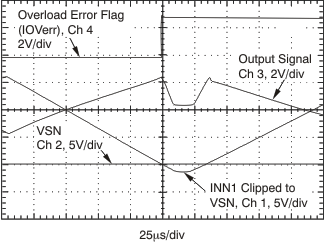
Overload conditions can vary widely. There are multiple points in an instrumentation amplifier that can be overloaded. During input overload, the PGA280 folds the output signal partially back as a result of the differential signal structure and summing, but the error flags indicate such fault conditions. The amplifier recovers safely after removing the overload condition, if the amplifier is within the specified operating range shown in Figure 69.
Avoid dynamic overload by using adequate signal filtering that reduces the input slew rate to that of the amplifier. Fast signal jumps produced from multiplexed signal sources or gain changes cannot normally be filtered, but in such situations, the current buffer (BUF) stage can be activated to prevent current flowing through the input into the protection clamp.
 Figure 69. Input Clipping: Negative Side