SLASEJ4C April 2017 – February 2023 PGA460
PRODUCTION DATA
- 1 Features
- 2 Applications
- 3 Description
- 4 Revision History
- 5 Pin Configuration and Functions
-
6 Specifications
- 6.1 Absolute Maximum Ratings
- 6.2 ESD Ratings
- 6.3 Recommended Operating Conditions
- 6.4 Thermal Information
- 6.5 Internal Supply Regulators Characteristics
- 6.6 Transducer Driver Characteristics
- 6.7 Transducer Receiver Characteristics
- 6.8 Analog to Digital Converter Characteristics
- 6.9 Digital Signal Processing Characteristics
- 6.10 Temperature Sensor Characteristics
- 6.11 High-Voltage I/O Characteristics
- 6.12 Digital I/O Characteristics
- 6.13 EEPROM Characteristics
- 6.14 Timing Requirements
- 6.15 Switching Characteristics
- 6.16 Typical Characteristics
-
7 Detailed Description
- 7.1 Overview
- 7.2 Functional Block Diagram
- 7.3
Feature Description
- 7.3.1 Power-Supply Block
- 7.3.2 Burst Generation
- 7.3.3 Analog Front-End
- 7.3.4 Digital Signal Processing
- 7.3.5 System Diagnostics
- 7.3.6
Interface Description
- 7.3.6.1 Time-Command Interface
- 7.3.6.2
USART Interface
- 7.3.6.2.1 USART Asynchronous Mode
- 7.3.6.2.2 One-Wire UART Interface
- 7.3.6.2.3 Ultrasonic Object Detection Through UART Operations
- 7.3.6.3 In-System IO-Pin Interface Selection
- 7.3.7 Echo Data Dump
- 7.3.8 Low-Power Mode
- 7.3.9 Transducer Time and Temperature Decoupling
- 7.3.10 Memory CRC Calculation
- 7.3.11 Temperature Sensor and Temperature Data-Path
- 7.3.12 TEST Pin Functionality
- 7.4 Device Functional Modes
- 7.5 Programming
- 7.6 Register Maps
- 8 Application and Implementation
- 9 Device and Documentation Support
- 10Mechanical, Packaging, and Orderable Information
Package Options
Mechanical Data (Package|Pins)
- PW|16
Thermal pad, mechanical data (Package|Pins)
Orderable Information
7.3.4.4 Ultrasonic Echo—Threshold Data Assignment
The PGA460 threshold assignments are organized in two presets: Preset1 and Preset2. Both of these presets have an independent memory map for threshold segment allocation. The PGA460 device supports up to 12 threshold segments for each preset defined by the threshold segment points (TSP) in the P1_THR_[0:15] registers for Preset1 and P2_THR_[0:15]registers for Preset2.
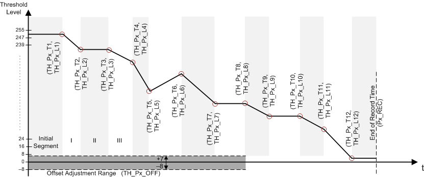
#X8043 shows an example of a threshold assignment.
 Figure 7-6 Threshold Assignment Example
As shown in #X8043, each TSP is described in the (time, level) format while Px is the preset number (P1 for Preset1, P2 for Preset2). Additionally, only the initial segment time parameter (TH_Px_T1) value is expressed in terms of absolute time, while all following TSP times (TH_Px_Tx parameters) are expressed as a delta time between the absolute time value of the previous TSP and the absolute time value of the current TSP. The level values of each TSP (TH_Px_Lx parameters) are all expressed in an absolute LSB-level value and are unrelated from each other. The TSP level threshold value at any given time moment is determined by the PGA460 device as a linear interpolation function between the two neighboring threshold segment points
As shown in #X8043, the initial segment has a constant threshold value determined by the TH_Px_L1 parameter until reaching the start of the first segment and also the 12th segment will have a constant threshold value determined by the TH_Px_L12 parameter until reaching the end of record time defined by the Px_REC parameter.
The TH_Px_L1 through TH_Px_L8 threshold parameters are 5-bits wide and the TH_Px_L9 through TH_Px_L12 parameters are 8-bits wide. These sizes help save memory space and at the same time allow higher resolution for long-range detection of weak echo signals in presence of noise while keeping the range constant across all TSPs. Because the TH_Px_L1 through TH_Px_L8 resolution is an 8 LSB, a threshold offset is defined to allow finer adjustment of the threshold map for short-range detection.
- All calculated values of TSP after adding offset, if negative, are clamped to 0 before linear interpolation which causes the slope of threshold curve to deviate from expected value.
- Both Preset1 and Preset2 threshold map parameters are protected by a CRC calculation algorithm (GUID-0EE0B425-DE2D-48BE-AA87-B1AD2F3EC245.html#X1155).
- At power up or wakeup from low power mode, all threshold registers (Px_THR_XX) and threshold CRC register (THR_CRC) are not initialized to the default value which causes a CRC error and sets THR_CRC_ERR bit to 1. This occurrence indicates to the MCU that the configuration is not loaded properly. Writing to threshold registers reruns CRC calculation and updates the error bit.