SLASEJ4C April 2017 – February 2023 PGA460
PRODUCTION DATA
- 1 Features
- 2 Applications
- 3 Description
- 4 Revision History
- 5 Pin Configuration and Functions
-
6 Specifications
- 6.1 Absolute Maximum Ratings
- 6.2 ESD Ratings
- 6.3 Recommended Operating Conditions
- 6.4 Thermal Information
- 6.5 Internal Supply Regulators Characteristics
- 6.6 Transducer Driver Characteristics
- 6.7 Transducer Receiver Characteristics
- 6.8 Analog to Digital Converter Characteristics
- 6.9 Digital Signal Processing Characteristics
- 6.10 Temperature Sensor Characteristics
- 6.11 High-Voltage I/O Characteristics
- 6.12 Digital I/O Characteristics
- 6.13 EEPROM Characteristics
- 6.14 Timing Requirements
- 6.15 Switching Characteristics
- 6.16 Typical Characteristics
-
7 Detailed Description
- 7.1 Overview
- 7.2 Functional Block Diagram
- 7.3
Feature Description
- 7.3.1 Power-Supply Block
- 7.3.2 Burst Generation
- 7.3.3 Analog Front-End
- 7.3.4 Digital Signal Processing
- 7.3.5 System Diagnostics
- 7.3.6
Interface Description
- 7.3.6.1 Time-Command Interface
- 7.3.6.2
USART Interface
- 7.3.6.2.1 USART Asynchronous Mode
- 7.3.6.2.2 One-Wire UART Interface
- 7.3.6.2.3 Ultrasonic Object Detection Through UART Operations
- 7.3.6.3 In-System IO-Pin Interface Selection
- 7.3.7 Echo Data Dump
- 7.3.8 Low-Power Mode
- 7.3.9 Transducer Time and Temperature Decoupling
- 7.3.10 Memory CRC Calculation
- 7.3.11 Temperature Sensor and Temperature Data-Path
- 7.3.12 TEST Pin Functionality
- 7.4 Device Functional Modes
- 7.5 Programming
- 7.6 Register Maps
- 8 Application and Implementation
- 9 Device and Documentation Support
- 10Mechanical, Packaging, and Orderable Information
Package Options
Mechanical Data (Package|Pins)
- PW|16
Thermal pad, mechanical data (Package|Pins)
Orderable Information
7.3.11 Temperature Sensor and Temperature Data-Path
The PGA460 device has an on-chip temperature sensor and a dedicated temperature data path for accurate temperature measurement. The output value is provided as an unsigned 8-bit number from –40°C to +125°C. The temperature sensor measurement can be used to adjust the variation of the transducer performance as the ambient temperature changes. The temperature measurement's sample and conversion time requires at least 100 us after the temperature measurement command is issued. Do not send other commands during this time to allow the temperature value to properly update.
The output of the temperature digital data path can be read by using the time-command interface of the UART interface. The value provided is related to the measured temperature as shown in #X250.
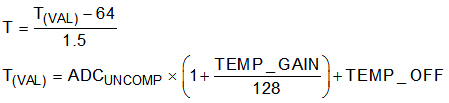
where
- T(VAL) is value read from the device using TCI or UART commands.
- T is the temperature.
- TEMP_GAIN and TEMP_OFF are signed values in the limits from –8 to +7.
Because the output value of T(VAL) after the calculation can result in a decimal number, the value is rounded-up to the closest integer value.
#X1446 shows the temperature digital data path, which has a 16-sample averager and a scaling block. The 16-sample averaging block averages 16 temperature measurements arriving at a rate of 1 sample/µs into one result to remove temperature measurement variations. The scaling block is used to adjust the Gain and the offset parameter to better calibrate the temperature sensor. These two parameters are programmed using TEMP_GAIN and TEMP_OFF bits in the TEMP_TRIM EEPROM register.
 Figure 7-39 Temperature-Sensor Signal Path
Before compensation (TEMP_GAIN bit set to 0, TEMP_OFF bit set to 0), T(VAL) is same the value converted by the ADC. As previously above, the user can compensate for variations in operating conditions (VPWR), board design, and configuration of the device by performing a two-temperature measurement and trim. After compensation, T(VAL) can be converted to an absolute temperature using #X250. As the VPWR is increased, power dissipation increases and the internal die temperature can be different from the ambient temperature. The temperature sensor always indicates the die temperature.
Without calibrating TEMP_GAIN and TEMP_OFF, the ambient temperature can be approximated from the die temperature reading using #T4793009-6
where
- RθJA (°C/W) is the Junction-to-ambient thermal resistance of 96.1°C/W.
- VPWR (V) is the input voltage.
- IVPWR_RX_ONLY (mA) is the supply current from VPWR pin during listen only mode of 12 mA.