SLOS412D April 2003 – November 2014 RC4580
PRODUCTION DATA.
- 1 Features
- 2 Applications
- 3 Description
- 4 Revision History
- 5 Pin Configuration and Functions
- 6 Specifications
- 7 Detailed Description
- 8 Application and Implementation
- 9 Power Supply Recommendations
- 10Layout
- 11Device and Documentation Support
- 12Mechanical, Packaging, and Orderable Information
Package Options
Refer to the PDF data sheet for device specific package drawings
Mechanical Data (Package|Pins)
- D|8
- P|8
- PW|8
Thermal pad, mechanical data (Package|Pins)
Orderable Information
6 Specifications
6.1 Absolute Maximum Ratings
over operating free-air temperature range (unless otherwise noted) (1)(1) Stresses beyond those listed under Absolute Maximum Ratings may cause permanent damage to the device. These are stress ratings only, which do not imply functional operation of the device at these or any other conditions beyond those indicated under Recommended Operating Conditions. Exposure to absolute-maximum-rated conditions for extended periods may affect device reliability.
6.2 Handling Ratings
| MIN | MAX | UNIT | |||
|---|---|---|---|---|---|
| Tstg | Storage temperature range | –60 | 125 | °C | |
| V(ESD) | Electrostatic discharge | Human body model (HBM), per ANSI/ESDA/JEDEC JS-001, all pins(1) | 0 | 1000 | V |
| Charged device model (CDM), per JEDEC specification JESD22-C101, all pins(2) | 0 | 1000 | |||
(1) JEDEC document JEP155 states that 500-V HBM allows safe manufacturing with a standard ESD control process.
(2) JEDEC document JEP157 states that 250-V CDM allows safe manufacturing with a standard ESD control process.
6.3 Recommended Operating Conditions
| MIN | MAX | UNIT | |||
|---|---|---|---|---|---|
| VCC+ | Supply voltage | 2 | 16 | V | |
| VCC– | –2 | –16 | |||
| VICR | Input common-mode voltage range | –13.5 | 13.5 | V | |
| TA | Operating free-air temperature | –40 | 125 | °C | |
6.4 Thermal Information
| THERMAL METRIC(1) | RC4580 | UNIT | ||
|---|---|---|---|---|
| D | PW | |||
| 8 PINS | 8 PINS | |||
| RθJA | Junction-to-ambient thermal resistance | 109 | 163 | °C/W |
| RθJC(top) | Junction-to-case (top) thermal resistance | 55.7 | 38 | |
| RθJB | Junction-to-board thermal resistance | 49 | 90.6 | |
| ψJT | Junction-to-top characterization parameter | 10.6 | 1.3 | |
| ψJB | Junction-to-board characterization parameter | 48.6 | 88.9 | |
| RθJC(bot) | Junction-to-case (bottom) thermal resistance | — | — | |
(1) For more information about traditional and new thermal metrics, see the IC Package Thermal Metrics application report, SPRA953.
6.5 Electrical Characteristics
VCC± = ±15 V, TA = –40°C to 125°C (unless otherwise noted)| PARAMETER | TEST CONDITIONS | MIN | TYP | MAX | UNIT | |
|---|---|---|---|---|---|---|
| VIO | Input offset voltage | RS = < 10 kΩ | 0.5 | 3 | mV | |
| IIO | Input offset current | 5 | 200 | nA | ||
| IIB | Input bias current | 100 | 500 | nA | ||
| AVD | Large-signal differential voltage amplification | RL ≥ 2 kΩ, VO = ±10 V | 90 | 110 | dB | |
| VCM | Output voltage swing | RL ≥ 2 kΩ | ±12 | ±13.5 | V | |
| VICR | Common-mode input voltage | ±12 | ±13.5 | V | ||
| CMRR | Common-mode rejection ratio | RS ≤ 10 kΩ | 80 | 110 | dB | |
| kSVR | Supply-voltage rejection ratio(1) | RS ≤ 10 kΩ | 80 | 110 | dB | |
| ICC | Total supply current (all amplifiers) | 6 | 9 | mA | ||
(1) Measured with VCC± varied simultaneously
6.6 Operating Characteristics
VCC± = ±15 V, TA = –40°C to 125°C (unless otherwise noted)| PARAMETER | TEST CONDITIONS | TYP | UNIT | |
|---|---|---|---|---|
| SR | Slew rate at unity gain | RL ≥ 2 kΩ | 5 | V/μs |
| GBW | Gain-bandwidth product | f = 10 kHz | 12 | MHz |
| THD | Total harmonic distortion | VO = 5 V, RL = 2 kΩ, f = 1 kHz, AVD = 20 dB | 0.0005% | |
| Vn | Equivalent input noise voltage | RIAA, RS ≤ 2.2 kΩ, 30-kHz LPF | 0.8 | μVrms |
6.7 Typical Characteristics
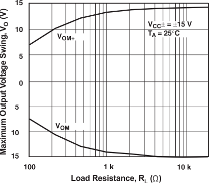 Figure 1. Maximum Output Voltage Swing vs Load Resistance
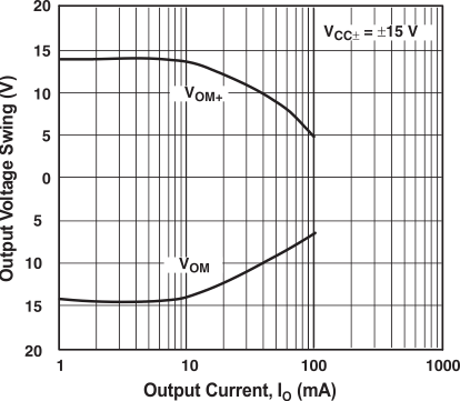 Figure 3. Output Voltage Swing vs Output Current
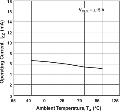 Figure 5. Operating Current vs Temperature
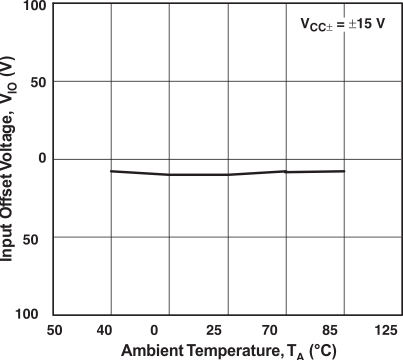 Figure 7. Input Offset Voltage vs Temperature
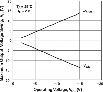 Figure 9. Maximum Output Voltage Swing vs Operating Voltage
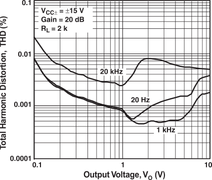 Figure 11. Total Harmonic Distortion vs Output Voltage
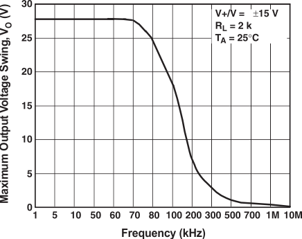 Figure 2. Maximum Ouput Voltage Swing vs Frequency
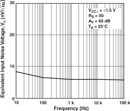 Figure 4. Equivalent Input Noise Voltage vs Frequency
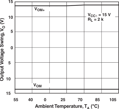 Figure 6. Output Voltage Swing vs Temperature
Figure 8. Input Bias Current vs Temperature
Figure 6. Output Voltage Swing vs Temperature
Figure 8. Input Bias Current vs Temperature
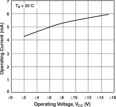 Figure 10. Operating Current vs Operating Voltage
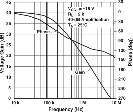 Figure 12. Voltage Gain, Phase vs Frequency