SBVS032I March 2002 – July 2022 REF3012 , REF3020 , REF3025 , REF3030 , REF3033 , REF3040
PRODUCTION DATA
- 1 Features
- 2 Applications
- 3 Description
- 4 Revision History
- 5 Device Comparison Table
- 6 Pin Configuration and Functions
- 7 Specifications
- 8 Detailed Description
- 9 Application and Implementation
- 10Power Supply Recommendations
- 11Layout
- 12Device and Documentation Support
- 13Mechanical, Packaging, and Orderable Information
Package Options
Mechanical Data (Package|Pins)
- DBZ|3
Thermal pad, mechanical data (Package|Pins)
Orderable Information
8.3.1 Supply Voltage
The REF30xx family of references features an extremely low dropout voltage. With the exception of the REF3012, which has a minimum supply requirement of 1.8 V, the REF30xx can be operated with a supply of only 1 mV above the output voltage in an unloaded condition. For loaded conditions, a typical dropout voltage versus load is shown on the front page.
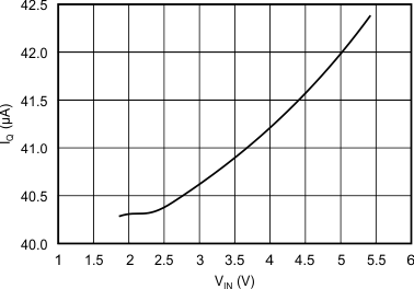
The REF30xx features a low quiescent current that is extremely stable over changes in both temperature and supply. The typical room temperature quiescent current is 42 μA, and the maximum quiescent current over temperature is just 59 μA. Additionally, the quiescent current typically changes less than 2.5 μA over the entire supply range, as shown in Figure 8-1.
Supply voltages below the specified levels can cause the REF30xx to momentarily draw currents greater than the typical quiescent current. Use a power supply with a fast rising edge and low output impedance to easily prevent this issue.
 Figure 8-1 Supply Current vs Supply Voltage