SBAS901C July   2018  – October 2020 REF34-Q1

PRODUCTION DATA  

  1. Features
  2. Applications
  3. Description
  4. Revision History
  5. Device Comparison Table
  6. Pin Configuration and Functions
    1. 6.1 Pin Functions
  7. Specifications
    1. 7.1 Absolute Maximum Ratings
    2. 7.2 ESD Ratings
    3. 7.3 Recommended Operating Conditions
    4. 7.4 Thermal Information
    5. 7.5 Electrical Characteristics
  8. Typical Characteristics
  9. Parameter Measurement Information
    1. 9.1 Solder Heat Shift
    2. 9.2 Long-Term Stability
    3. 9.3 Thermal Hysteresis
    4. 9.4 Power Dissipation
    5. 9.5 Noise Performance
  10. 10Detailed Description
    1. 10.1 Overview
    2. 10.2 Functional Block Diagram
    3. 10.3 Feature Description
      1. 10.3.1 Supply Voltage
      2. 10.3.2 Low Temperature Drift
      3. 10.3.3 Load Current
    4. 10.4 Device Functional Modes
      1. 10.4.1 EN Pin
  11. 11Application and Implementation
    1. 11.1 Application Information
    2. 11.2 Typical Applications
      1. 11.2.1 Basic Voltage Reference Connection
        1. 11.2.1.1 Design Requirements
        2. 11.2.1.2 Detailed Design Procedure
          1. 11.2.1.2.1 Input and Output Capacitors
          2. 11.2.1.2.2 4-Wire Kelvin Connections
          3. 11.2.1.2.3 VIN Slew Rate Considerations
          4. 11.2.1.2.4 Shutdown/Enable Feature
        3. 11.2.1.3 Application Curves
      2. 11.2.2 Advanced Driver Assistance Systems (ADAS) Microcontroller Connection
        1. 11.2.2.1 Basic Voltage Reference Connection
        2. 11.2.2.2 Design Requirements
        3. 11.2.2.3 Detailed Design Procedure
        4. 11.2.2.4 Enable Feature in ADAS
  12. 12Power Supply Recommendations
  13. 13Layout
    1. 13.1 Layout Guidelines
    2. 13.2 Layout Example
  14. 14Device and Documentation Support
    1. 14.1 Documentation Support
      1. 14.1.1 Related Documentation
    2. 14.2 Receiving Notification of Documentation Updates
    3. 14.3 Support Resources
    4. 14.4 Trademarks
    5. 14.5 Electrostatic Discharge Caution
    6. 14.6 Glossary
  15. 15Mechanical, Packaging, and Orderable Information

Package Options

Mechanical Data (Package|Pins)
Thermal pad, mechanical data (Package|Pins)
Orderable Information

Power Dissipation

The REF34-Q1 voltage references are capable of source and sink up to 10 mA of load current across the rated input voltage range. However, when used in applications subject to high ambient temperatures, the input voltage and load current must be carefully monitored to ensure that the device does not exceeded its maximum power dissipation rating. The maximum power dissipation of the device can be calculated with Equation 2:
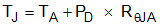
Equation 2. GUID-82261879-F79D-4A9D-B822-ADEE08CDE322-low.gif

where

  • PD is the device power dissipation
  • TJ is the device junction temperature
  • TA is the ambient temperature
  • RθJA is the package (junction-to-air) thermal resistance

Because of this relationship, acceptable load current in high temperature conditions may be less than the maximum current-sourcing capability of the device. In no case should the device be operated outside of its maximum power rating because doing so can result in premature failure or permanent damage to the device.