SBAS804F September   2017  – June 2021 REF3425 , REF3430 , REF3433 , REF3440 , REF3450

PRODUCTION DATA  

  1. Features
  2. Applications
  3. Description
  4. Revision History
  5. Device Comparison Table
  6. Pin Configuration and Functions
  7. Specifications
    1. 7.1 Absolute Maximum Ratings
    2. 7.2 ESD Ratings
    3. 7.3 Recommended Operating Conditions
    4. 7.4 Thermal Information
    5. 7.5 Electrical Characteristics
    6. 7.6 Typical Characteristics
  8. Parameter Measurement Information
    1. 8.1 Solder Heat Shift
    2. 8.2 Long-Term Stability
    3. 8.3 Thermal Hysteresis
    4. 8.4 Power Dissipation
    5. 8.5 Noise Performance
  9. Detailed Description
    1. 9.1 Overview
    2. 9.2 Functional Block Diagram
    3. 9.3 Feature Description
      1. 9.3.1 Supply Voltage
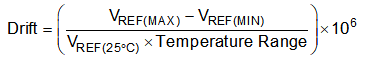
      2. 9.3.2 Low Temperature Drift
      3. 9.3.3 Load Current
    4. 9.4 Device Functional Modes
      1. 9.4.1 EN Pin
      2. 9.4.2 Negative Reference Voltage
  10. 10Application and Implementation
    1. 10.1 Application Information
    2. 10.2 Typical Application: Basic Voltage Reference Connection
      1. 10.2.1 Design Requirements
      2. 10.2.2 Detailed Design Procedure
        1. 10.2.2.1 Input and Output Capacitors
        2. 10.2.2.2 4-Wire Kelvin Connections
        3. 10.2.2.3 VIN Slew Rate Considerations
        4. 10.2.2.4 Shutdown/Enable Feature
      3. 10.2.3 Application Curves
  11. 11Power Supply Recommendations
  12. 12Layout
    1. 12.1 Layout Guidelines
    2. 12.2 Layout Example
  13. 13Device and Documentation Support
    1. 13.1 Documentation Support
      1. 13.1.1 Related Documentation
    2. 13.2 Receiving Notification of Documentation Updates
    3. 13.3 Support Resources
    4. 13.4 Trademarks
    5. 13.5 Electrostatic Discharge Caution
    6. 13.6 Glossary
  14. 14Mechanical, Packaging, and Orderable Information

Package Options

Mechanical Data (Package|Pins)
Thermal pad, mechanical data (Package|Pins)
Orderable Information

Low Temperature Drift

The REF34xx is designed for minimal drift error, which is defined as the change in output voltage over temperature. The drift is calculated using the box method, as described by Equation 3. For this equation, VREF is VOUT which is the output voltage seen at the junction of OUT_F and OUT_S.

Equation 3. GUID-20210405-CA0I-HV5Z-CPFM-6H5P01QLFHZX-low.gif