SBOS410K june 2007 – june 2023 REF5010 , REF5020 , REF5025 , REF5030 , REF5040 , REF5045 , REF5050
PRODUCTION DATA
- 1
- 1 Features
- 2 Applications
- 3 Description
- 4 Revision History
- 5 Device Comparison Table
- 6 Pin Configuration and Functions
- 7 Specifications
- 8 Parameter Measurement Information
- 9 Detailed Description
- 10Applications and Implementation
- 11Power Supply Recommendations
- 12Layout
- 13Device and Documentation Support
- 14Mechanical, Packaging, and Orderable Information
Package Options
Mechanical Data (Package|Pins)
Thermal pad, mechanical data (Package|Pins)
- DGK|8
Orderable Information
9.3.5 Long-Term Stability
Due to aging and environmental effects, all semiconductor devices experience physical changes of the semiconductor die and the packaging material over time. These changes and the associated package stress on the die cause the output voltage in precision voltage references to deviate over time. The value of such change is specified in the data sheet by a parameter called the long-term stability (also known as the long-term drift (LTD)). Equation 4 shows how LTD is calculated. Note that the LTD value is positive if the output voltage drifts higher over time and negative if the voltage drifts lower over time. Figure 7-23 through Figure 7-30 show the drift of the output voltage for REF50xx over the first 4000 operating hours.
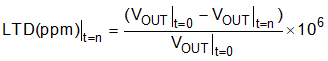
where
- LTD(ppm)|t=n = long-term stability (in units of ppm)
- VOUT|t=0 = output voltage at time = 0 hr
- VOUT|t=n = output voltage at time = n hr