SLLSF98 December 2018 SN55HVD233-SEP
PRODUCTION DATA.
- 1 Features
- 2 Applications
- 3 Description
- 4 Revision History
- 5 Description (continued)
- 6 Pin Configuration and Functions
-
7 Specifications
- 7.1 Absolute Maximum Ratings
- 7.2 ESD Ratings
- 7.3 Recommended Operating Conditions
- 7.4 Thermal Information
- 7.5 Driver Electrical Characteristics
- 7.6 Receiver Electrical Characteristics
- 7.7 Driver Switching Characteristics
- 7.8 Receiver Switching Characteristics
- 7.9 Device Switching Characteristics
- 7.10 Typical Characteristics
- 8 Parameter Measurement Information
- 9 Detailed Description
- 10Application and Implementation
- 11Power Supply Recommendations
- 12Layout
- 13Device and Documentation Support
- 14Mechanical, Packaging, and Orderable Information
Package Options
Mechanical Data (Package|Pins)
- D|8
Thermal pad, mechanical data (Package|Pins)
Orderable Information
12.1.2 CAN Termination
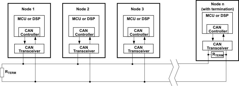
The ISO11898 standard specifies the interconnect to be a twisted pair cable (shielded or unshielded) with 120-Ω characteristic impedance (ZO). Use resistors equal to the characteristic impedance of the line to terminate both ends of the cable to prevent signal reflections. Keep unterminated drop lines (stubs) connecting nodes to the bus as short as possible to minimize signal reflections. The termination may be on the cable or in a node, but if nodes may be removed from the bus, the termination must be carefully placed so that it is not removed from the bus.
 Figure 33. Typical CAN Bus
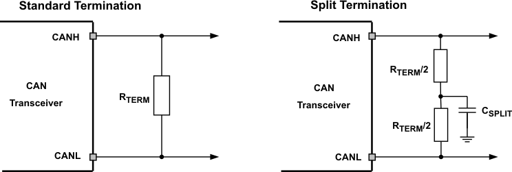
 Termination is typically a 120-Ω resistor at each end of the bus. If filtering and stabilization of the common mode voltage of the bus is desired, then the user may use split termination (see Figure 34). Split termination uses two 60-Ω resistors with a capacitor in the middle of these resistors to ground. Split termination improves the electromagnetic emissions behavior of the network by eliminating fluctuations in the bus common mode voltages at the start and end of message transmissions.
Take care with the power ratings of the termination resistors used, especially for the worst-case condition (if a system power supply is shorted across the termination resistance to ground). In most cases, under the worst-case condition, much higher current passes through the termination resistance than the CAN transceiver's current limit.
 Figure 34. CAN Bus Termination Concepts