SLLSEJ8E June 2014 – April 2019 SN65HVD1470 , SN65HVD1471 , SN65HVD1473 , SN65HVD1474 , SN65HVD1476 , SN65HVD1477
PRODUCTION DATA.
- 1 Features
- 2 Applications
- 3 Description
- 4 Revision History
- 5 Device Comparison Table
- 6 Pin Configuration and Functions
-
7 Specifications
- 7.1 Absolute Maximum Ratings
- 7.2 ESD Ratings
- 7.3 Recommended Operating Conditions
- 7.4 Thermal Information — D Packages
- 7.5 Thermal Information — DGS and DGK Packages
- 7.6 Power Dissipation
- 7.7 Electrical Characteristics
- 7.8 Switching Characteristics — 400 kbps
- 7.9 Switching Characteristics — 20 Mbps
- 7.10 Switching Characteristics — 50 Mbps
- 7.11 Typical Characteristics
- 8 Parameter Measurement Information
- 9 Detailed Description
- 10Application and Implementation
- 11Power Supply Recommendations
- 12Layout
- 13Device and Documentation Support
- 14Mechanical, Packaging, and Orderable Information
Package Options
Mechanical Data (Package|Pins)
Thermal pad, mechanical data (Package|Pins)
- D|14
Orderable Information
6 Pin Configuration and Functions
SN65HVD1471, SN65HVD1474, SN65HVD1477
8-Pin SOIC, D Package, and 8-Pin MSOP, DGK Package
(Top View)
SN65HVD1471
8-Pin SOIC, D Package

Pin Functions — SOIC-8 and MSOP-8
| PIN | TYPE | DESCRIPTION | |
|---|---|---|---|
| NAME | NO. | ||
| VCC | 1 | Supply | 3-V to 3.6-V supply |
| R | 2 | Digital output | Receive data output |
| D | 3 | Digital input | Driver data input |
| GND | 4 | Reference potential | Local device ground |
| Y | 5 | Bus output | Digital bus output, Y (Complementary to Z) |
| Z | 6 | Bus output | Digital bus output, Z (Complementary to Y) |
| B | 7 | Bus input | Digital bus input, B (Complementary to A) |
| A | 8 | Bus input | Digital bus input, A (Complementary to B) |
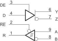
SN65HVD1470, SN65HVD1473, SN65HVD1476
10-Pin MSOP, DGS Package
(Top View)
SN65HVD1470
10-Pin MSOP, DGS Package

Pin Functions — MSOP–10
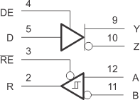
SN65HVD1470, SN65HVD1473, SN65HVD1476
14-Pin SOIC, D Package
(Top View)
NC = no internal connection
SN65HVD1470
10-Pin MSOP, DGS Package

Pin Functions — SOIC-14
| PIN | TYPE | DESCRIPTION | |
|---|---|---|---|
| NAME | NO. | ||
| NC | 1 | No connect | Not connected |
| 8 | |||
| R | 2 | Digital output | Receive data output |
| RE | 3 | Digital input | Receive enable Low |
| DE | 4 | Digital input | Driver enable High |
| D | 5 | Digital input | Driver data input |
| GND | 6(1) | Reference potential | Local device ground |
| 7(1) | |||
| Y | 9 | Bus output | Digital bus output, Y (Complementary to Z) |
| Z | 10 | Bus output | Digital bus output, Z (Complementary to Y) |
| B | 11 | Bus input | Digital bus input, B (Complementary to A) |
| A | 12 | Bus input | Digital bus input, A (Complementary to B) |
| VCC | 13(2) | Supply | 3-V to 3.6-V supply |
| 14(2) | |||
(1) Pin 6 and pin 7 are connected internally.
(2) Pin 13 and pin 14 are connected internally.