SLLSEJ8E June 2014 – April 2019 SN65HVD1470 , SN65HVD1471 , SN65HVD1473 , SN65HVD1474 , SN65HVD1476 , SN65HVD1477
PRODUCTION DATA.
- 1 Features
- 2 Applications
- 3 Description
- 4 Revision History
- 5 Device Comparison Table
- 6 Pin Configuration and Functions
-
7 Specifications
- 7.1 Absolute Maximum Ratings
- 7.2 ESD Ratings
- 7.3 Recommended Operating Conditions
- 7.4 Thermal Information — D Packages
- 7.5 Thermal Information — DGS and DGK Packages
- 7.6 Power Dissipation
- 7.7 Electrical Characteristics
- 7.8 Switching Characteristics — 400 kbps
- 7.9 Switching Characteristics — 20 Mbps
- 7.10 Switching Characteristics — 50 Mbps
- 7.11 Typical Characteristics
- 8 Parameter Measurement Information
- 9 Detailed Description
- 10Application and Implementation
- 11Power Supply Recommendations
- 12Layout
- 13Device and Documentation Support
- 14Mechanical, Packaging, and Orderable Information
Package Options
Mechanical Data (Package|Pins)
Thermal pad, mechanical data (Package|Pins)
Orderable Information
10.2.2 Detailed Design Procedure
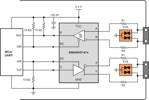
In order to protect bus nodes against high-energy transients, the implementation of external transient protection devices is therefore necessary. Figure 37 shows a protection circuit against 16-kV ESD, 4-kV EFT, and 1-kV surge transients.
 Figure 37. Transient Protection Against ESD, EFT, and Surge transients
 Table 6. Bill of Materials
| DEVICE | FUNCTION | ORDER NUMBER | MANUFACTURER |
|---|---|---|---|
| XCVR | 3.3-V, full-duplex RS-485 transceiver | SN65HVD147xD | TI |
| R1 | 10-Ω, pulse-proof thick-film resistor | CRCW0603010RJNEAHP | Vishay |
| R2 | |||
| TVS | Bidirectional 400-W transient suppressor | CDSOT23-SM712 | Bourns |