SGLS367E September 2006 – September 2015 SN65HVD30-EP , SN65HVD33-EP
PRODUCTION DATA.
- 1 Features
- 2 Applications
- 3 Description
- 4 Revision History
- 5 Pin Configuration and Functions
-
6 Specifications
- 6.1 Absolute Maximum Ratings
- 6.2 ESD Ratings
- 6.3 Recommended Operating Conditions
- 6.4 Thermal Information
- 6.5 Electrical Characteristics: Driver
- 6.6 Electrical Characteristics: Receiver
- 6.7 Switching Characteristics: Driver
- 6.8 Switching Characteristics: Receiver
- 6.9 Receiver Equalization Characteristics
- 6.10 Dissipation Ratings
- 6.11 Typical Characteristics
- 7 Parameter Measurement Information
- 8 Detailed Description
- 9 Application and Implementation
- 10Power Supply Recommendations
- 11Layout
- 12Device and Documentation Support
- 13Mechanical, Packaging, and Orderable Information
Package Options
Mechanical Data (Package|Pins)
- D|8
Thermal pad, mechanical data (Package|Pins)
- D|8
Orderable Information
8 Detailed Description
8.1 Overview
The SN65HVD3x-EP devices are low-power, full-duplex RS-485 transceivers available in three speed grades suitable for data transmission of 1 Mbps, 5 Mbps, and 50 Mbps.
The SN65HVD30, SN65HVD31, and SN65HVD32 devices are fully enabled with no external enabling pins. The SN65HVD33, SN65HVD34, and SN65HVD35 devices have active-high driver enables and active-low receiver enables. A standby current of less than 1 µA can be achieved by disabling both driver and receiver.
8.2 Functional Block Diagram
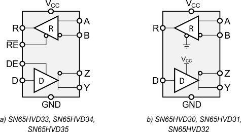
8.3 Feature Description
8.3.1 Low-Power Standby Mode
When both the driver and receiver are disabled (DE is low and RE is high), the device is in standby mode. If the enable inputs are in this state for less than 60 ns, the device does not enter standby mode. This guards against inadvertently entering standby mode during driver or receiver enabling. The device in standby mode only when the enable inputs are held in this state for 300 ns or more. In this low-power standby mode, most internal circuitry is powered down, and the supply current is typically less than 1 nA. When either the driver or the receiver is re-enabled, the internal circuitry becomes active.
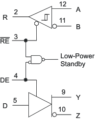 Figure 22. Low-Power Standby Logic Diagram
If only the driver is re-enabled (DE transitions to high) the driver outputs are driven according to the D input after the enable times given by tPZH2 and tPZL2 in the driver switching characteristics. If the D input is open when the driver is enabled, the driver output defaults to Y high and Z low, in accordance with the driver-failsafe feature.
If only the receiver is re-enabled (RE transitions to low) the receiver output is driven according to the state of the bus inputs (A and B) after the enable times given by tPZH2 and tPZL2 in the receiver switching characteristics. If there is no valid state on the bus the receiver responds as described in the failsafe operation section.
If both the receiver and driver are re-enabled simultaneously, the receiver output is driven according to the state of the bus inputs (A and B) and the driver output is driven according to the D input. Note that the state of the active driver affects the inputs to the receiver. Therefore, the receiver outputs are valid as soon as the driver outputs are valid.
8.3.2 Driver Output Current Limiting
The RS-485 standard (ANSI/TIA/EIA-485-A or equivalently ISO 8482) specifies a 250-mA driver output current limit to prevent damage caused by data contention on the bus. That applies in the event that two or more transceivers drive the bus to opposing states at the same time. The SN65HVD3x-EP family of devices includes current-limiting circuitry that prevents damage under these conditions.
NOTE
This current limit prevents damage during the bus contention, but the logic state of the bus can be indeterminate as specified by the standard, so communication errors can occur.
In a specific combination of circumstances, a condition can occur in which current through the bus pin exceeds the 250-mA limit. This combination of conditions is not normally included in RS-485 applications:
- Loading capacitance on the pin is less than 500 pF
- The bus pin is directly connected to a voltage more negative than –1 V
- The device is supplied with VCC equal to or greater than 3.3 V
- The driver is enabled
- The bus pin is driving to the logic high state
In these specific conditions, the normal current-limit circuitry and thermal-shutdown circuitry does not limit or shutdown the current flow. If the current is allowed to continue, the device heats up in a localized area near the driver outputs, and the device can be damaged.
Typical RS-485 twisted-pair cable has a capacitance of approximately 50 pF/meter. Therefore, it is expected that 10 meters of cable can provide sufficient capacitance to prevent this latch-up condition.
The –7 to +12-V common mode range specified by RS-485 is intended to allow communication between transceivers separated by significant distances when ground offsets may occur due to temporary current surges, electrical noise, and so on. Under those circumstances, the inherent cable needed to connect separated transceivers ensures that the conditions previously listed do not occur. For a transceiver separated by only a short cable length or backplane applications, it is unusual for there to be a steady-state negative common-mode voltage. It is possible for a negative power supply to be shorted to the bus lines due to miswiring or cable damage; however, this is a different root cause fault, and robust devices such as the SN65HVD178x family should be used for surviving power supply or miswiring faults.
The 250-mA current limit in the RS-485 standard is intended to prevent damage caused by data contention on the bus; that is, in the event that two or more transceivers drive the bus to different states at the same time. These devices are not damaged under these conditions because all RS-485 drivers have output impedance sufficient to prevent the direct connection condition stated previously. Typical RS-485 driver output impedance is on the order of 10 Ω to 30 Ω.
8.3.3 Hot-Plugging
These devices are designed to operate in hot swap or hot pluggable applications. Key features for hot-pluggable applications are:
- Power-up
- Power-down glitch-free operation
- Default disabled input/output pins
- Receiver failsafe
As shown in Figure 9, an internal power-on reset circuit keeps the driver outputs in a high-impedance state until the supply voltage has reached a level at which the device reliably operates. This ensures that no spurious bits are transmitted on the bus pin outputs as the power supply turns on or turns off.
As shown in the Device Functional Modes, the enable inputs have the feature of default disable on both the driver enable and receiver enable. This ensures that the device neither drives the bus nor reports data on the R pin until the associated controller actively drives the enable pins.
8.3.4 Receiver Failsafe
The differential receivers of the SN65HVD3x-EP family are failsafe to invalid bus states caused by:
- Open bus conditions such as a disconnected connector
- Shorted bus conditions such as cable damage shorting the twisted-pair together
- Idle bus conditions that occur when no driver on the bus is actively driving
In any of these cases, the differential receiver outputs a failsafe logic high state so that the output of the receiver is not indeterminate.
Receiver failsafe is accomplished by offsetting the receiver thresholds such that the input indeterminate range does not include zero volts differential. In order to comply with the RS-422 and RS-485 standards, the receiver output must output a high when the differential input VID is more positive than 200 mV, and must output a low when VID is more negative than –200 mV. The receiver parameters which determine the failsafe performance are VIT+, VIT–, and VHYS (the separation between VIT+ and VIT–. As shown in the Electrical Characteristics: Receiver table, differential signals more negative than –200 mV always cause a low receiver output, and differential signals more positive than 200 mV always cause a high receiver output.
When the differential input signal is close to zero, it is still above the VIT+ threshold, and the receiver output is high. Only when the differential input is more than VHYS below VIT+ does the receiver output transition to a low state. Therefore, the noise immunity of the receiver inputs during a bus fault conditions includes the receiver hysteresis value (VHYS) as well as the value of VIT+.
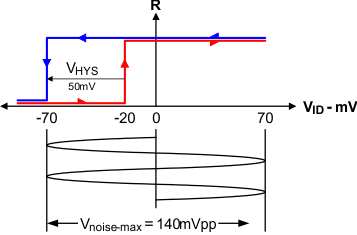 Figure 23. SN65HVD30-35 Noise Immunity Under Bus Fault Conditions
8.3.5 Safe Operation With Bus Contention
These devices incorporate a driver current limit of 250 mA across the RS-485 common-mode range of –7 V to +12 V. As stated in the Application Guidelines for TIA/EIA-485-A
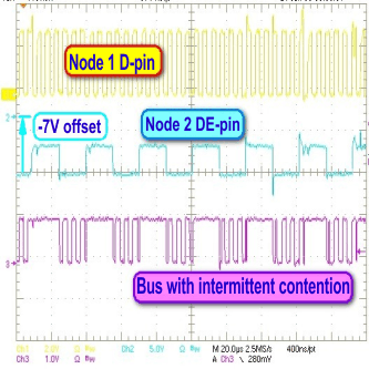
Figure 24 shows a 2-node system to demonstrate bus contention by forcing both drivers to be active in opposing states.
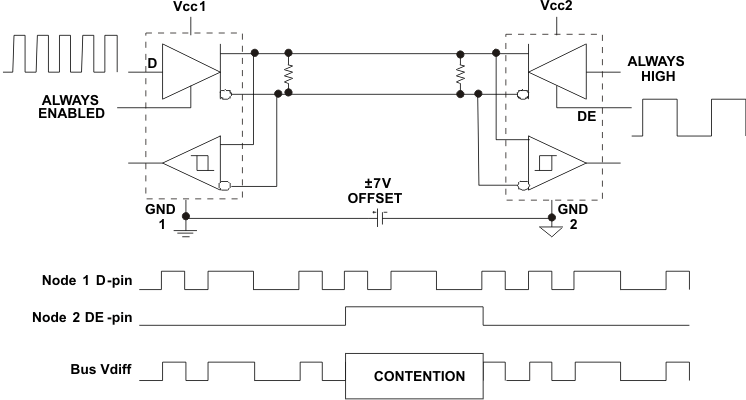 Figure 24. Bus Contention Example
Figure 25 shows typical operation in a bus contention event. The bottom trace illustrates how the SN65HVD33 device at Node 1 continues normal operation after a contention event between the two drivers with a –7-V ground offset on Node 2. This illustrates how the SN65HVD3x-EP family of devices operates robustly in spite of bus contention faults, even with large common-mode offsets.
8.4 Device Functional Modes
Table 3-Table 6 list the functional modes of the S65HVDxx Devices.
Table 3. SN65HVD33, SN65HVD34, SN65HVD35 Driver
| INPUTS | OUTPUTS | ||
|---|---|---|---|
| D | DE | Y | Z |
| H | H | H | L |
| L | H | L | H |
| X | L or open | Z | Z |
| Open | H | L | H |
Table 4. SN65HVD33, SN65HVD34, SN65HVD35 Receiver
| DIFFERENTIAL INPUTS VID = V(A) – V(B) |
ENABLE RE |
OUTPUT R |
|---|---|---|
| VID ≤ –0.2 V | L | L |
| –0.2 V < VID < –0.02 V | L | — |
| –0.02 V ≤ VID | L | H |
| X | H or open | Z |
| Open Circuit | L | H |
| Idle circuit | L | H |
| Short Circuit, V(A) = V(B) | L | H |
Table 6. SN65HVD30, SN65HVD31, SN65HVD32 Receiver
| DIFFERENTIAL INPUTS VID = V(A) – V(B) |
OUTPUT R |
|---|---|
| VID ≤ –0.2 V | L |
| –0.02 V ≤ VID | H |
| Open Circuit | H |
| Idle circuit | H |
| Short Circuit, V(A) = V(B) | H |
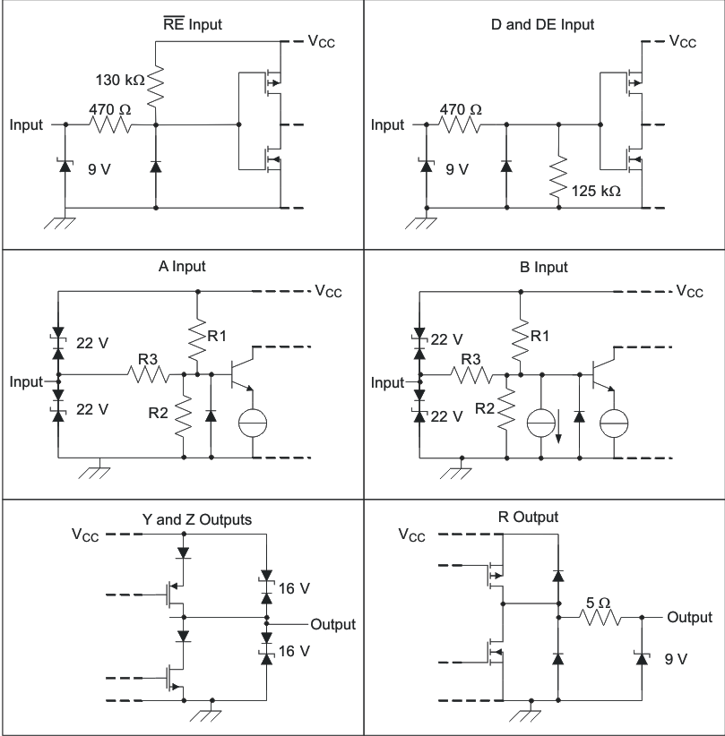 Figure 26. Equivalent Input and Output Schematic Diagrams
