SLLSE94C September 2011 – March 2015 SN65HVD62
PRODUCTION DATA.
- 1 Features
- 2 Applications
- 3 Description
- 4 Block Diagram
- 5 Revision History
- 6 Pin Configuration and Functions
- 7 Specifications
- 8 Parameter Measurement Information
- 9 Detailed Description
- 10Application and Implementation
- 11Device and Documentation Support
- 12Mechanical, Packaging, and Orderable Information
Package Options
Mechanical Data (Package|Pins)
- RGT|16
Thermal pad, mechanical data (Package|Pins)
- RGT|16
Orderable Information
1 Features
- Supply Ranging From 3V to 5.5V
- Independent Logic Supply of 1.6V to 5.5V
- Wide Input Dynamic Range of –15dBm to +5dBm for Receiver
- Power Delivered by the Driver to the Coax can be Adjusted From 0dBm to +6dBm
- AISG Compliant Output Emission Profile
- Low-power Standby Mode
- Direction Control Output for RS-485 Bus Arbitration
- Supports up to 115 kbps Signaling
- Integrated Active Bandpass Filter with Center Frequency at 2.176MHz
- 3mm × 3mm 16-Pin QFN Package
2 Applications
- AISG – Interface for Antenna Line Devices
- Tower Mounted Amplifiers (TMA)
- General Modem Interfaces
3 Description
These transceivers modulate and demodulate signals between the logic (baseband) and a frequency suitable for long coaxial media.
The HVD62 is an integrated AISG transceiver designed to be compliant with Antenna Interface Standards Group v2.0 specification.
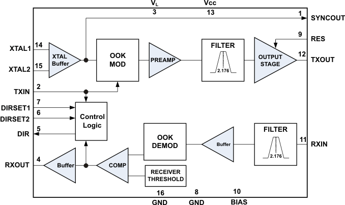
The HVD62 receiver integrates an active bandpass filter to enable demodulation of signals even in the presence of spurious frequency components. The filter has a 2.176 MHz center frequency.
The transmitter supports adjustable output power levels varying from +0dBm to +6dBm delivered to the 50 Ω coax cable. The HVD62 transmitter is compliant with the spectrum emission requirement provided by the AISG standard.
A direction control output is provided which facilitates bus arbitration for an RS-485 interface. These devices integrate an oscillator input for a crystal, and also accept standard clock inputs to the oscillator.
Device Information(1)
| PART NUMBER | PACKAGE | BODY SIZE (NOM) |
|---|---|---|
| SN65HVD62 | VQFN (16) | 3.00 mm x 3.00 mm |
- For all available packages, see the orderable addendum at the end of the data sheet.
4 Block Diagram
