SLLSFE2 June   2019 SN65HVDA1040B-Q1

PRODUCTION DATA.  

  1. Features
  2. Applications
  3. Description
    1.     Block Diagram
  4. Revision History
  5. Pin Configuration and Functions
    1.     Pin Functions
  6. Specifications
    1. 6.1 Absolute Maximum Ratings
    2. 6.2 ESD Ratings
    3. 6.3 Recommended Operating Conditions
    4. 6.4 Thermal Information
    5. 6.5 Electrical Characteristics
    6. 6.6 Power Dissipation Characteristics
    7. 6.7 Switching Characteristics
    8. 6.8 Typical Characteristics
  7. Parameter Measurement Information
  8. Detailed Description
    1. 8.1 Overview
    2. 8.2 Functional Block Diagram
    3. 8.3 Feature Description
      1. 8.3.1 Operating Modes
        1. 8.3.1.1 Bus States by Mode
        2. 8.3.1.2 Normal Mode
        3. 8.3.1.3 Standby Mode and RXD Wake-Up Request
      2. 8.3.2 Protection Features
        1. 8.3.2.1 TXD Dominant State Time-Out
        2. 8.3.2.2 Thermal Shutdown
        3. 8.3.2.3 Undervoltage Lockout and Unpowered Device
    4. 8.4 Device Functional Modes
  9. Application and Implementation
    1. 9.1 Application Information
      1. 9.1.1 Using With 3.3-V Microcontrollers
      2. 9.1.2 Using SPLIT With Split Termination
    2. 9.2 Typical Application
      1. 9.2.1 Design Requirements
        1. 9.2.1.1 Bus Loading, Length, and Number of Nodes
        2. 9.2.1.2 CAN Termination
        3. 9.2.1.3 Loop Propagation Delay
      2. 9.2.2 Detailed Design Procedure
        1. 9.2.2.1 Transient Voltage Suppresser (TVS) Diodes
      3. 9.2.3 Application Curves
  10. 10Power Supply Recommendations
  11. 11Layout
    1. 11.1 Layout Guidelines
    2. 11.2 Layout Example
    3. 11.3 ESD Protection
  12. 12Device and Documentation Support
    1. 12.1 Documentation Support
      1. 12.1.1 Related Documentation
    2. 12.2 Receiving Notification of Documentation Updates
    3. 12.3 Community Resources
    4. 12.4 Trademarks
    5. 12.5 Electrostatic Discharge Caution
    6. 12.6 Glossary
  13. 13Mechanical, Packaging, and Orderable Information

Package Options

Mechanical Data (Package|Pins)
Thermal pad, mechanical data (Package|Pins)
Orderable Information

Bus States by Mode

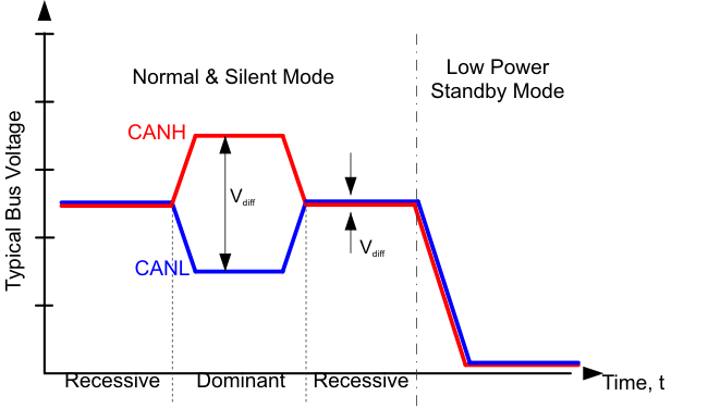
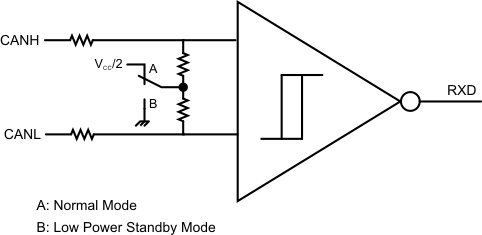
The CAN bus has three valid states during powered operation depending on the mode of the device. In normal mode the bus may be dominant (logic low) where the bus lines are driven differentially apart or recessive (logic high) where the bus lines are biased to VCC/2 through the high-ohmic internal input resistors RIN of the receiver. The third state is low-power standby mode where the bus lines is biased to GND through the high-ohmic internal input resistors RIN of the receiver.
SN65HVDA1040B-Q1 bus_states_physical_bit_lls804.gif
Figure 16. Bus States (Physical Bit Representation)
SN65HVDA1040B-Q1 simplified_common_mode_bias_lls804.gif
Figure 17. Simplified Common-Mode Bias and Receiver Implementation