SLLSEU5 December 2016 SN65LBC175A-EP
PRODUCTION DATA.
- 1 Features
- 2 Applications
- 3 Description
- 4 Revision History
- 5 Pin Configuration and Functions
- 6 Specifications
- 7 Parameter Measurement Information
- 8 Detailed Description
- 9 Application and Implementation
- 10Power Supply Recommendations
- 11Layout
- 12Device and Documentation Support
- 13Mechanical, Packaging, and Orderable Information
Package Options
Mechanical Data (Package|Pins)
- D|16
Thermal pad, mechanical data (Package|Pins)
Orderable Information
1 Features
- Designed for TIA/EIA-485, TIA/EIA-422 and
ISO 8482 Applications - Signaling Rates (1) Exceeding 50 Mbps
- Fail-Safe in Bus Short-Circuit, Open-Circuit, and Idle-Bus Conditions
- ESD Protection on Bus Inputs Exceeds 6 kV
- Common-Mode Bus Input Range –7 V to 12 V
- Propagation Delay Times < 18 ns
- Low Standby Power Consumption < 32 µA
- Pin-Compatible Upgrade for MC3486, DS96F175, LTC489, and SN75175
2 Applications
- Supports Defense, Aerospace, and Medical Applications
- Controlled Baseline
- One Assembly and Test Site
- One Fabrication Site
- Extended Product Life Cycle
- Extended Product-Change Notification
- Product Traceability
3 Description
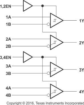
The SN65LBC175A-EP is a quadruple differential line receiver with 3-state outputs, designed for TIA/EIA-485 (RS-485), TIA/EIA-422 (RS-422), and ISO 8482 (Euro RS-485) applications.
This device is optimized for balanced multipoint bus communication at data rates up to and exceeding 50 million bits per second. The transmission media may be twisted-pair cables, printed-circuit board traces, or backplanes. The ultimate rate and distance of data transfer is dependent upon the attenuation characteristics of the media and the noise coupling to the environment.
The receiver operates over a wide range of positive and negative common-mode input voltages, and features ESD protection to 6 kV, making it suitable for high-speed multipoint data transmission applications in harsh environments. These devices are designed using LinBiCMOS®, facilitating low power consumption and robustness.
Two EN inputs provide pair-wise enable control, or these can be tied together externally to enable all four drivers with the same signal.
.
Device Information(1)
| PART NUMBER | PACKAGE | BODY SIZE (NOM) |
|---|---|---|
| SN65LBC175A-EP | SOIC (16) | 9.90 mm × 3.90 mm |
- For all available packages, see the orderable addendum at the end of the data sheet.
Logic Diagram
