SLLS573D December 2003 – December 2015 SN65MLVD200A , SN65MLVD202A , SN65MLVD204A , SN65MLVD205A
PRODUCTION DATA.
- 1 Features
- 2 Applications
- 3 Description
- 4 Revision History
- 5 Device Comparison Table
- 6 Pin Configuration and Functions
-
7 Specifications
- 7.1 Absolute Maximum Ratings
- 7.2 ESD Ratings
- 7.3 Recommended Operating Conditions
- 7.4 Thermal Information
- 7.5 Electrical Characteristics
- 7.6 Electrical Characteristics - Driver
- 7.7 Electrical Characteristics - Receiver
- 7.8 Electrical Characteristics - BUS Input and Output
- 7.9 Switching Characteristics - Driver
- 7.10 Switching Characteristics - Receiver
- 7.11 Typical Characteristics
- 8 Parameter Measurement Information
- 9 Detailed Description
-
10Application and Implementation
- 10.1 Application Information
- 10.2
Typical Application
- 10.2.1 Design Requirements
- 10.2.2
Detailed Design Procedure
- 10.2.2.1 Supply Voltage
- 10.2.2.2 Supply Bypass Capacitance
- 10.2.2.3 Driver Input Voltage
- 10.2.2.4 Driver Output Voltage
- 10.2.2.5 Termination Resistors
- 10.2.2.6 Receiver Input Signal
- 10.2.2.7 Receiver Input Threshold (Failsafe)
- 10.2.2.8 Receiver Output Signal
- 10.2.2.9 Interconnecting Media
- 10.2.2.10 PCB Transmission Lines
- 10.2.3 Application Curves
- 11Power Supply Recommendations
- 12Layout
- 13Device and Documentation Support
- 14Mechanical, Packaging, and Orderable Information
Package Options
Refer to the PDF data sheet for device specific package drawings
Mechanical Data (Package|Pins)
- D|14
Thermal pad, mechanical data (Package|Pins)
- D|14
Orderable Information
9 Detailed Description
9.1 Overview
The SN65MLVD20xA family of devices are multipoint-low-voltage differential (M-LVDS) line drivers and receivers that are optimized to operate at signaling rates up to 100 Mbps. All parts comply with the multipoint low-voltage differential signaling (M-LVDS) standard TIA/EIA-899. These circuits are similar to their TIA/EIA-644 standard compliant LVDS counterparts with added features to address multipoint applications. The driver output has been designed to support multipoint buses presenting loads as low as 30 Ω and incorporates controlled transition times to allow for stubs off of the backbone transmission line.
These devices have Type-1 and Type-2 receivers that detect the bus state with as little as 50 mV (for Type-1) or 150 mV (for Type-2) of differential input voltage over a common-mode voltage range of –1 V to 3.4 V. The Type-1 receivers exhibit 25 mV of differential input voltage hysteresis to prevent output oscillations with slowly changing signals or loss of input. Type-2 receivers include an offset threshold to provide a known output state under open-circuit and bus-idle fault conditions.
9.2 Functional Block Diagram
 Figure 25. Logic Diagrams (Positive Logic)
9.3 Feature Description
9.3.1 Power-On Reset
This family of devices operates and meets all the specified performance requirements for supply voltages in the range of 3 V to 3.6 V. When the supply voltage drops below 1.5 V (or is turning on and has not yet reached 1.5 V), power-on reset circuitry sets the driver output to a high-impedance state.
9.3.2 ESD Protection
The bus terminals of the SN65MLVD20xA devices possess on-chip ESD protection against ±8-kV human body model (HBM) and ±8 kV.
9.4 Device Functional Modes
9.4.1 Device Function Tables
Table 3. Type-1 Receiver (SN65MLVD200A)(1)
| INPUTS | OUTPUT | |
|---|---|---|
| VID = VA - VB | RE | R |
| VID ≥ 50 mV | L | H |
| –50 mV < VID < 50 mV | L | ? |
| VID ≤ –50 mV | L | L |
| X | H | Z |
| X | Open | Z |
Table 4. Type-2 Receiver (SN65MLVD204A)(1)
| INPUTS | OUTPUT | |
|---|---|---|
| VID = VA - VB | RE | R |
| VID ≥ 150 mV | L | H |
| 50 mV < VID < 150 mV | L | ? |
| VID ≤ 50 mV | L | L |
| X | H | Z |
| X | Open | Z |
Table 5. Driver(1)
| INPUTS | ENABLE | OUTPUTS | |
|---|---|---|---|
| D | DE | A | B |
| L | H | L | H |
| H | H | H | L |
| Open | H | L | H |
| X | Open | Z | Z |
| X | L | Z | Z |
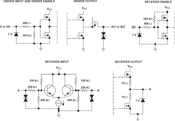
9.4.2 Equivalent Input and Output Schematic Diagrams
