SLLS573D December 2003 – December 2015 SN65MLVD200A , SN65MLVD202A , SN65MLVD204A , SN65MLVD205A
PRODUCTION DATA.
- 1 Features
- 2 Applications
- 3 Description
- 4 Revision History
- 5 Device Comparison Table
- 6 Pin Configuration and Functions
-
7 Specifications
- 7.1 Absolute Maximum Ratings
- 7.2 ESD Ratings
- 7.3 Recommended Operating Conditions
- 7.4 Thermal Information
- 7.5 Electrical Characteristics
- 7.6 Electrical Characteristics - Driver
- 7.7 Electrical Characteristics - Receiver
- 7.8 Electrical Characteristics - BUS Input and Output
- 7.9 Switching Characteristics - Driver
- 7.10 Switching Characteristics - Receiver
- 7.11 Typical Characteristics
- 8 Parameter Measurement Information
- 9 Detailed Description
-
10Application and Implementation
- 10.1 Application Information
- 10.2
Typical Application
- 10.2.1 Design Requirements
- 10.2.2
Detailed Design Procedure
- 10.2.2.1 Supply Voltage
- 10.2.2.2 Supply Bypass Capacitance
- 10.2.2.3 Driver Input Voltage
- 10.2.2.4 Driver Output Voltage
- 10.2.2.5 Termination Resistors
- 10.2.2.6 Receiver Input Signal
- 10.2.2.7 Receiver Input Threshold (Failsafe)
- 10.2.2.8 Receiver Output Signal
- 10.2.2.9 Interconnecting Media
- 10.2.2.10 PCB Transmission Lines
- 10.2.3 Application Curves
- 11Power Supply Recommendations
- 12Layout
- 13Device and Documentation Support
- 14Mechanical, Packaging, and Orderable Information
Package Options
Refer to the PDF data sheet for device specific package drawings
Mechanical Data (Package|Pins)
- D|8
Thermal pad, mechanical data (Package|Pins)
- D|8
Orderable Information
10 Application and Implementation
NOTE
Information in the following applications sections is not part of the TI component specification, and TI does not warrant its accuracy or completeness. TI’s customers are responsible for determining suitability of components for their purposes. Customers should validate and test their design implementation to confirm system functionality.
10.1 Application Information
The SN65MLVD20xA family of devices are multipoint line drivers and receivers. The functionality of these devices is simple, yet extremely flexible, thus leading to their use in designs ranging from wireless base stations to desktop computers.
10.2 Typical Application
Figure 26 shows a multipoint configuration. In a multipoint configuration, many transmitters and many receivers can be interconnected on one transmission line. The key difference compared to multidrop is the presence of two or more drivers. Such a situation creates contention issues that must not be addressed with point-to-point or multidrop systems. Multipoint operation allows for bidirectional, half-duplex communication over one balanced media pair. To support the location of the various drivers throughout the transmission line, double termination of the transmission line is now necessary.
The major challenge that system designers encounter are the impedance discontinuities that device loading and device connections (stubs) introduce on the common bus. Matching the impedance of the loaded bus and using signal drivers with controlled signal edges are the keys to error-free signal transmissions in multipoint topologies.
10.2.1 Design Requirements
For this design example, use the parameters listed in Table 6.
Table 6. Design Parameters
| PARAMETERS | VALUES |
|---|---|
| Driver supply voltage | 3 V to 3.6 V |
| Driver input voltage | 0.8 V to 3.3 V |
| Driver signaling rate | DC to 100 Mbps |
| Interconnect characteristic impedance (differential) | 100 Ω |
| Termination resistance | 100 Ω |
| Number of receiver nodes | 2 to 32 |
| Receiver supply voltage | 3 V to 3.6 V |
| Receiver input voltage | 0 to (VCC – 0.8) V |
| Receiver signaling rate | DC to 100 Mbps |
| Ground shift between driver and receiver | ±1 V |
10.2.2 Detailed Design Procedure
10.2.2.1 Supply Voltage
The SN65MLVD20xA devices are operated from one supply. The SN65MLVD20xA devices can support operation with a supply as low as 3 V and as high as 3.6 V.
10.2.2.2 Supply Bypass Capacitance
Bypass capacitors play a key role in power distribution circuitry. At low frequencies, power supply offers very low-impedance paths between its terminals. However, as higher frequency currents propagate through power traces, the source is often incapable of maintaining a low-impedance path to ground. Bypass capacitors are used to address this shortcoming. Usually, large bypass capacitors (10 μF to 1000 μF) at the board level do a good job up into the kHz range. Due to their size and length of their leads, large capacitors tend to have large inductance values at the switching frequencies. To solve this problem, smaller capacitors (in the nF to μF range) must be installed locally next to the integrated circuit.
Multilayer ceramic chip or surface-mount capacitors (size 0603 or 0805) minimize lead inductances of bypass capacitors in high-speed environments, because their lead inductance is about 1 nH. For comparison purposes, a typical capacitor with leads has a lead inductance around 5 nH.
The value of the bypass capacitors used locally with M-LVDS chips can be determined by Equation 1 and Equation 2, according to High Speed Digital Design – A Handbook of Black Magic by Howard Johnson and Martin Graham (1993). A conservative rise time of 4 ns and a worst-case change in supply current of 100 mA covers the whole range of M-LVDS devices offered by Texas Instruments. In this example, the maximum power supply noise tolerated is 100 mV; however, this figure varies depending on the noise budget available for the design.


Figure 27 shows a configuration that lowers lead inductance and covers intermediate frequencies between the board-level capacitor (>10 µF) and the value of capacitance found above (0.004 µF). Place the smallest value of capacitance as close as possible to the chip.
 Figure 27. Recommended M-LVDS Bypass Capacitor Layout
10.2.2.3 Driver Input Voltage
The input stage accepts LVTTL signals. The driver will operate with a decision threshold of approximately 1.4 V.
10.2.2.4 Driver Output Voltage
The driver outputs a steady state common mode voltage of 1 V with a differential signal of 540 V under nominal conditions.
10.2.2.5 Termination Resistors
An M-LVDS communication channel employs a current source driving a transmission line that is terminated with two resistive loads. These loads serve to convert the transmitted current into a voltage at the receiver input. To ensure good signal integrity, the termination resistors must be matched to the characteristic impedance of the transmission line. The designer must ensure that the termination resistors are within 10% of the nominal media characteristic impedance. If the transmission line is targeted for 100-Ω impedance, the termination resistors must be between 90 Ω and 110 Ω. The line termination resistors are typically placed at the ends of the transmission line.
10.2.2.6 Receiver Input Signal
The M-LVDS receivers herein comply with the M-LVDS standard and correctly determine the bus state. These devices have Type-1 and Type-2 receivers that detect the bus state with as little as 50 mV of differential voltage over the common mode range of –1 V to 3.4 V.
10.2.2.7 Receiver Input Threshold (Failsafe)
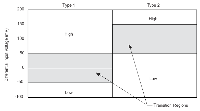
The M-LVDS standard defines a Type-1 and a Type-2 receiver. Type-1 receivers have differential input voltage thresholds near zero volts. Type-2 receivers have differential input voltage thresholds offset from 0 V to detect the absence of a voltage difference. The impact to receiver output by the offset input can be seen in Table 7 and Figure 28.
Table 7. Receiver Input Voltage Threshold Requirements
| RECEIVER TYPE | OUTPUT LOW | OUTPUT HIGH |
|---|---|---|
| Type 1 | –2.4 V ≤ VID ≤ –0.05 V | 0.05 V ≤ VID ≤ 2.4 V |
| Type 2 | –2.4 V ≤ VID ≤ 0.05 V | 0.15 V ≤ VID ≤ 2.4 V |
 Figure 28. Expanded Graph of Receiver Differential Input Voltage Showing Transition Region
10.2.2.8 Receiver Output Signal
Receiver outputs comply with LVTTL output voltage standards when the supply voltage is within the range of 3 V to 3.6 V.
10.2.2.9 Interconnecting Media
The physical communication channel between the driver and the receiver may be any balanced, paired metal conductors that meet the requirements of the M-LVDS standard—the key points are included in the following. The interconnecting media may be a twisted pair, twinax, flat ribbon cable, or PCB traces.
The nominal characteristic impedance of the interconnect must be between 100 Ω and 120 Ω with variation no more than 10% (90 Ω to 132 Ω).
10.2.2.10 PCB Transmission Lines
The LVDS Owner's Manual Design Guide, 4th Edition (SNLA187), Figure 29 depicts several transmission line structures commonly used in printed-circuit boards (PCBs). Each structure consists of a signal line and a return path with uniform cross-section along its length. A microstrip is a signal trace on the top (or bottom) layer that is separated by a dielectric layer from its return path in a ground or power plane. A stripline is a signal trace in the inner layer, with a dielectric layer in between a ground plane above and below the signal trace. The dimensions of the structure along with the dielectric material properties determine the characteristic impedance of the transmission line, which is also called controlled-impedance transmission line.
When two signal lines are placed close together, they form a pair of coupled transmission lines. Figure 29 shows examples of edge-coupled microstrips and edge-coupled or broad-side-coupled striplines. When excited by differential signals, the coupled transmission line is referred to as a differential pair. The characteristic impedance of each line is called odd-mode impedance. The sum of the odd-mode impedances of each line is the differential impedance of the differential pair. In addition to the trace dimensions and dielectric material properties, the spacing between the two traces determines the mutual coupling and impacts the differential impedance. When the two lines are immediately adjacent (for example, if S is less than 2 × W) the differential pair is called a tightly-coupled differential pair. To maintain constant differential impedance along the length, it is important to keep the trace width and spacing uniform along the length and to maintain good symmetry between the two lines.
 Figure 29. Controlled-Impedance Transmission Lines
10.2.3 Application Curves

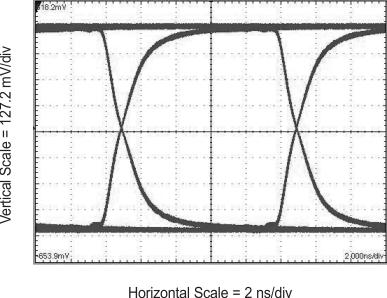
| 100 Mbps | 215 –1 PRBS | RL = 50 Ω |

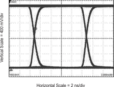
| 100 Mbps | 215 –1 PRBS | CL = 15 pF |
