SLLS573D December 2003 – December 2015 SN65MLVD200A , SN65MLVD202A , SN65MLVD204A , SN65MLVD205A
PRODUCTION DATA.
- 1 Features
- 2 Applications
- 3 Description
- 4 Revision History
- 5 Device Comparison Table
- 6 Pin Configuration and Functions
-
7 Specifications
- 7.1 Absolute Maximum Ratings
- 7.2 ESD Ratings
- 7.3 Recommended Operating Conditions
- 7.4 Thermal Information
- 7.5 Electrical Characteristics
- 7.6 Electrical Characteristics - Driver
- 7.7 Electrical Characteristics - Receiver
- 7.8 Electrical Characteristics - BUS Input and Output
- 7.9 Switching Characteristics - Driver
- 7.10 Switching Characteristics - Receiver
- 7.11 Typical Characteristics
- 8 Parameter Measurement Information
- 9 Detailed Description
-
10Application and Implementation
- 10.1 Application Information
- 10.2
Typical Application
- 10.2.1 Design Requirements
- 10.2.2
Detailed Design Procedure
- 10.2.2.1 Supply Voltage
- 10.2.2.2 Supply Bypass Capacitance
- 10.2.2.3 Driver Input Voltage
- 10.2.2.4 Driver Output Voltage
- 10.2.2.5 Termination Resistors
- 10.2.2.6 Receiver Input Signal
- 10.2.2.7 Receiver Input Threshold (Failsafe)
- 10.2.2.8 Receiver Output Signal
- 10.2.2.9 Interconnecting Media
- 10.2.2.10 PCB Transmission Lines
- 10.2.3 Application Curves
- 11Power Supply Recommendations
- 12Layout
- 13Device and Documentation Support
- 14Mechanical, Packaging, and Orderable Information
Package Options
Refer to the PDF data sheet for device specific package drawings
Mechanical Data (Package|Pins)
- D|8
Thermal pad, mechanical data (Package|Pins)
- D|8
Orderable Information
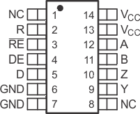
6 Pin Configuration and Functions
D Package
8-Pin SOIC
Top View

D Package
14-Pin SOIC
Top View

Pin Functions
| PIN | TYPE | DESCRIPTION | ||
|---|---|---|---|---|
| NAME | SOIC-8 | SOIC-14 | ||
| A | 6 | 12 | I/O | Differential I/O |
| B | 7 | 11 | I/O | Differential I/O |
| D | 4 | 5 | I | Driver input |
| DE | 3 | 4 | I | Driver enable pin: High = Enable, Low = Disable |
| GND | 5 | 6, 7 | Power | Supply ground |
| NC | — | 1, 8 | NC | No internal connection |
| R | 1 | 2 | O | Receiver output |
| RE | 2 | 3 | I | Receiver enable pin: High = Disable, Low = Enable |
| VCC | 8 | 13, 14 | Power | Power supply, 3.3 V |
| Y | — | 9 | I/O | Differential I/O |
| Z | — | 10 | I/O | Differential I/O |