SLLSEX9A December 2016 – February 2020 SN65MLVD206B
PRODUCTION DATA.
- 1 Features
- 2 Applications
- 3 Description
- 4 Revision History
- 5 Pin Configuration and Functions
-
6 Specifications
- Table 1. Absolute Maximum Ratings
- Table 2. ESD Ratings
- Table 3. Recommended Operating Conditions
- Table 4. Thermal Information
- Table 5. Electrical Characteristics
- Table 6. Electrical Characteristics – Driver
- Table 7. Electrical Characteristics – Receiver
- Table 8. Electrical Characteristics – BUS Input and Output
- Table 9. Switching Characteristics – Driver
- Table 10. Switching Characteristics – Receiver
- 6.1 Typical Characteristics
- 7 Parameter Measurement Information
- 8 Detailed Description
-
9 Application and Implementation
- 9.1 Application Information
- 9.2
Typical Application
- 9.2.1 Multipoint Communications
- 9.2.2 Design Requirements
- 9.2.3
Detailed Design Procedure
- 9.2.3.1 Supply Voltage
- 9.2.3.2 Supply Bypass Capacitance
- 9.2.3.3 Driver Input Voltage
- 9.2.3.4 Driver Output Voltage
- 9.2.3.5 Termination Resistors
- 9.2.3.6 Receiver Input Signal
- 9.2.3.7 Receiver Input Threshold (Failsafe)
- 9.2.3.8 Receiver Output Signal
- 9.2.3.9 Interconnecting Media
- 9.2.3.10 PCB Transmission Lines
- 9.2.4 Application Curves
- 10Power Supply Recommendations
- 11Layout
- 12Device and Documentation Support
- 13Mechanical, Packaging, and Orderable Information
Package Options
Mechanical Data (Package|Pins)
- D|8
Thermal pad, mechanical data (Package|Pins)
Orderable Information
7 Parameter Measurement Information
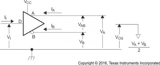 Figure 2. Driver Voltage and Current Definitions
A. All resistors are 1% tolerance.
Figure 3. Differential Output Voltage Test Circuit 
A. All input pulses are supplied by a generator having the following characteristics: tr or tf≤ 1 ns, pulse frequency = 1 MHz, duty cycle = 50 ± 5%.
B. C1, C2 and C3 include instrumentation and fixture capacitance within 2 cm of the D.U.T. and are ±20%.
C. R1 and R2 are metal film, surface mount, ±1%, and located within 2 cm of the D.U.T.
D. The measurement of VOS(PP) is made on test equipment with a -3 dB bandwidth of at least 1 GHz.
Figure 4. Test Circuit and Definitions for the Driver Common-Mode Output Voltage 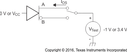 Figure 5. Driver Short-Circuit Test Circuit
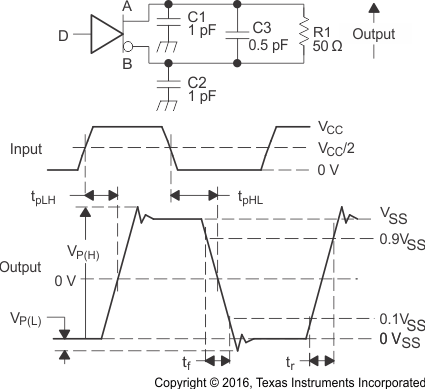
A. All input pulses are supplied by a generator having the following characteristics: tr or tf≤ 1 ns, frequency = 1 MHz, duty cycle = 50 ± 5%.
B. C1, C2, and C3 include instrumentation and fixture capacitance within 2 cm of the D.U.T. and are ±20%.
C. R1 is a metal film, surface mount, and 1% tolerance and located within 2 cm of the D.U.T.
D. The measurement is made on test equipment with a -3 dB bandwidth of at least 1 GHz.
Figure 6. Driver Test Circuit, Timing, and Voltage Definitions for the Differential Output Signal 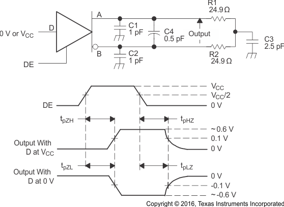
A. All input pulses are supplied by a generator having the following characteristics: tr or tf≤ 1 ns, frequency = 1 MHz, duty cycle = 50 ± 5%.
B. C1, C2, C3, and C4 includes instrumentation and fixture capacitance within 2 cm of the D.U.T. and are ±20%.
C. R1 and R2 are metal film, surface mount, and 1% tolerance and located within 2 cm of the D.U.T.
D. The measurement is made on test equipment with a -3 dB bandwidth of at least 1 GHz.
Figure 7. Driver Enable and Disable Time Circuit and Definitions 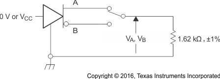 Figure 8. Maximum Steady State Output Voltage
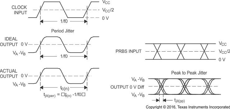
A. All input pulses are supplied by an Agilent 81250 Stimulus System.
B. The measurement is made on a TEK TDS6604 running TDSJIT3 application software
C. Period jitter is measured using a 100 MHz 50 ±1% duty cycle clock input.
D. Peak-to-peak jitter is measured using a 200 Mbps 215–1 PRBS input.
Figure 9. Driver Jitter Measurement Waveforms 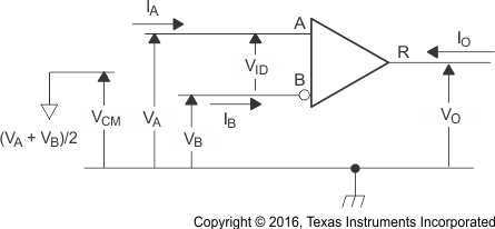 Figure 10. Receiver Voltage and Current Definitions
 Table 11. Type-2 Receiver Input Threshold Test Voltages
| APPLIED VOLTAGES | RESULTING DIFFERENTIAL
INPUT VOLTAGE |
RESULTING COMMON-
MODE INPUT VOLTAGE |
RECEIVER
OUTPUT(1) |
|
|---|---|---|---|---|
| VIA | VIB | VID | VIC | |
| 2.400 | 0.000 | 2.400 | 1.200 | H |
| 0.000 | 2.400 | –2.400 | 1.200 | L |
| 3.475 | 3.325 | 0.150 | 3.4 | H |
| 3.425 | 3.375 | 0.050 | 3.4 | L |
| –0.925 | –1.075 | 0.150 | –1 | H |
| –0.975 | –1.025 | 0.050 | –1 | L |
(1) H= high level, L = low level, output state assumes receiver is enabled (RE = L)
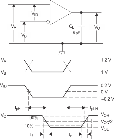
A. All input pulses are supplied by a generator having the following characteristics: tr or tf ≤ 1 ns, frequency = 1 MHz, duty cycle = 50 ± 5%. CL is a combination of a 20%-tolerance, low-loss ceramic, surface-mount capacitor and fixture capacitance within 2 cm of the D.U.T.
B. The measurement is made on test equipment with a –3 dB bandwidth of at least 1 GHz.
Figure 11. Receiver Timing Test Circuit and Waveforms 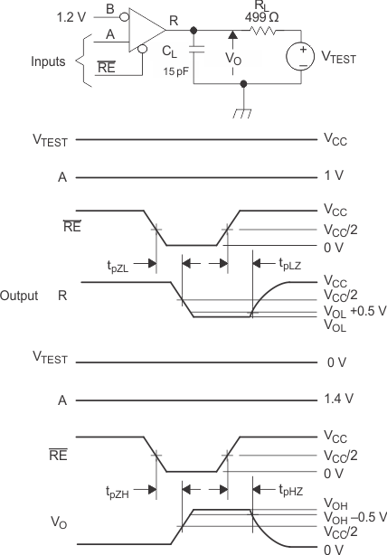
A. All input pulses are supplied by a generator having the following characteristics: tr or tf ≤ 1 ns, frequency = 1 MHz, duty cycle = 50 ± 5%.
B. RL is 1% tolerance, metal film, surface mount, and located within 2 cm of the D.U.T.
C. CL is the instrumentation and fixture capacitance within 2 cm of the DUT and ±20%.
Figure 12. Receiver Enable and Disable Time Test Circuit and Waveforms 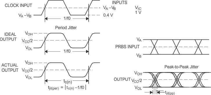
A. All input pulses are supplied by an Agilent 8304A Stimulus System.
B. The measurement is made on a TEK TDS6604 running TDSJIT3 application software
C. Period jitter is measured using a 10 MHz 50 ±1% duty cycle clock input.
D. Peak-to-peak jitter is measured using a 200 Mbps 215-1 PRBS input.
Figure 13. Receiver Jitter Measurement Waveforms