SCES551E February 2004 – November 2015 SN74AVC16T245
PRODUCTION DATA.
- 1 Features
- 2 Applications
- 3 Description
- 4 Revision History
- 5 Description (continued)
- 6 Pin Configuration and Functions
-
7 Specifications
- 7.1 Absolute Maximum Ratings
- 7.2 ESD Ratings
- 7.3 Recommended Operating Conditions
- 7.4 Thermal Information
- 7.5 Electrical Characteristics
- 7.6 Switching Characteristics: VCCA = 1.2 V
- 7.7 Switching Characteristics: VCCA = 1.5 V ± 0.1 V
- 7.8 Switching Characteristics: VCCA = 1.8 V ± 0.15 V
- 7.9 Switching Characteristics: VCCA = 2.5 V ± 0.2 V
- 7.10 Switching Characteristics: VCCA = 3.3 V ± 0.3 V
- 7.11 Operating Characteristics
- 7.12 Typical Characteristics
- 8 Parameter Measurement Information
- 9 Detailed Description
- 10Application and Implementation
- 11Power Supply Recommendations
- 12Layout
- 13Device and Documentation Support
- 14Mechanical, Packaging, and Orderable Information
Package Options
Mechanical Data (Package|Pins)
Thermal pad, mechanical data (Package|Pins)
Orderable Information
1 Features
- Control Inputs VIH/VIL Levels Are Referenced to VCCA Voltage
- VCC Isolation Feature – If Either VCC Input Is at GND, Both Ports Are in the High-Impedance State
- Overvoltage-Tolerant Inputs and Outputs Allow Mixed-Voltage-Mode Data Communications
- Fully Configurable Dual-Rail Design Allows Each Port to Operate Over the Full 1.2 V to 3.6 V Power-Supply Range
- Ioff Supports Partial-Power-Down Mode Operation
- I/Os Are 4.6 V Tolerant
- Maximum Data Rates
- 380 Mbps (1.8 V to 3.3 V Level-Shifting)
- 200 Mbps (<1.8 V to 3.3 V Level-Shifting)
- 200 Mbps (Level-Shifting to 2.5 V or 1.8 V)
- 150 Mbps (Level-Shifting to 1.5 V)
- 100 Mbps (Level-Shifting to 1.2 V)
- Latch-Up Performance Exceeds 100 mA Per JESD 78, Class II
- ESD Protection Exceeds JESD 22
- 8000-V Human-Body Model (A114-A)
- 200-V Machine Model (A115-A)
- 1000-V Charged-Device Model (C101)
2 Applications
- Personal Electronics
- Industrial
- Enterprise
- Telecom
3 Description
This 16-bit noninverting bus transceiver uses two separate configurable power-supply rails. The SN74AVC16T245 device is optimized to operate with VCCA/VCCB set at 1.4 V to 3.6 V. The device is operational with VCCA/VCCB as low as 1.2 V. The A port is designed to track VCCA. VCCA accepts any supply voltage from 1.2 V to 3.6 V. The B port is designed to track VCCB. VCCB accepts any supply voltage from 1.2 V to 3.6 V. This allows for universal low-voltage bidirectional translation between any of the 1.2-V, 1.5-V, 1.8-V, 2.5-V, and 3.3-V voltage nodes.
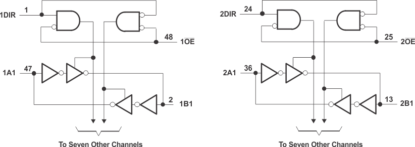
The SN74AVC16T245 device is designed for asynchronous communication between data buses. The device transmits data from the A bus to the B bus or from the B bus to the A bus, depending on the logic level at the direction-control (DIR) input. The output-enable (OE) input can be used to disable the outputs so the buses effectively are isolated.
The SN74AVC16T245 control pins (1DIR, 2DIR, 1OE, and 2OE) are supplied by VCCA.
Device Information(1)
| PART NUMBER | PACKAGE | BODY SIZE (NOM) |
|---|---|---|
| SN74AVC16T245 | TSSOP (48) | 12.50 mm × 6.10 mm |
| TVSOP (48) | 9.70 mm × 4.40 mm | |
| BGA MICROSTAR JUNIOR (56) |
7.00 mm × 4.50 mm |
- For all available packages, see the orderable addendum at the end of the data sheet.
Logic Diagram (Positive Logic)
