SCES692D June 2008 – February 2016 SN74AVC2T245
PRODUCTION DATA.
- 1 Features
- 2 Applications
- 3 Description
- 4 Revision History
- 5 Pin Configuration and Functions
-
6 Specifications
- 6.1 Absolute Maximum Ratings
- 6.2 ESD Ratings
- 6.3 Recommended Operating Conditions
- 6.4 Thermal Information
- 6.5 Electrical Characteristics
- 6.6 Switching Characteristics: VCCA = 1.2 V
- 6.7 Switching Characteristics: VCCA = 1.5 V ± 0.1 V
- 6.8 Switching Characteristics: VCCA = 1.8 V ± 0.15 V
- 6.9 Switching Characteristics: VCCA = 2.5 V ± 0.2 V
- 6.10 Switching Characteristics: VCCA = 3.3 V ± 0.3 V
- 6.11 Operating Characteristics
- 6.12 Typical Characteristics
- 7 Parameter Measurement Information
- 8 Detailed Description
- 9 Application and Implementation
- 10Power Supply Recommendations
- 11Layout
- 12Device and Documentation Support
- 13Mechanical, Packaging, and Orderable Information
Package Options
Mechanical Data (Package|Pins)
- RSW|10
Thermal pad, mechanical data (Package|Pins)
Orderable Information
8 Detailed Description
8.1 Overview
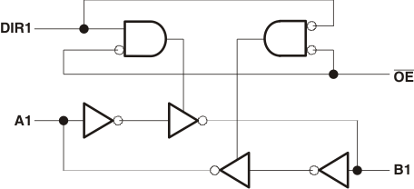
The SN74AVC2T245 is a dual-bit, dual-supply noninverting bidirectional voltage level translation. Pins A and control pins (DIR and OE) are supported by VCCA and pins B are supported by VCCB. The A port can accept I/O voltages ranging from 1.2 V to 3.6 V, while the B port can accept I/O voltages from 1.2 V to 3.6 V. A high on DIR allows data transmission from A to B and a low on DIR allows data transmission from B to A when OE is set to low. When OE is set to high, both A and B are in the high-impedance state.
This device is fully specified for partial-power-down applications using off output current (Ioff).
The VCC isolation feature ensures that if either VCC input is at GND, both ports are put in a high-impedance state.
8.2 Functional Block Diagram
 Figure 4. Logic Diagram (Positive Logic)
8.3 Feature Description
8.3.1 Fully Configurable Dual-Rail Design Allows Each Port to Operate Over the Full
1.2 V to 3.6 V Power-Supply Range
Both VCCA and VCCB can be supplied at any voltage from 1.2 V to 3.6 V making the device suitable for translating between any of the low voltage nodes (1.2 V, 1.8 V, 2.5 V, and 3.3 V).
8.3.2 Partial-Power-Down Mode Operation
This device is fully specified for partial-power-down applications using off output current (Ioff). The Ioff circuitry will prevent backflow current by disabling I/O output circuits when device is in partial power-down mode.
8.3.3 VCC Isolation
The VCC isolation feature ensures that if either VCCA or VCCB are at GND, both ports will be in a high-impedance state (IOZ). This prevents false logic levels from being presented to either bus.
8.4 Device Functional Modes
The SN74AVC2T245 is a voltage level translator that can operate from1.2 V to 3.6 V (VCCA) and 1.2 V to 3.6 V (VCCB). The signal translation requires direction control and output enable control. The table below enlists the operation of the part for the respective states of the control inputs.
Table 1. Function Table(1) (Each Transceiver)
| CONTROL INPUTS | OUTPUT CIRCUITS | OPERATION | ||
|---|---|---|---|---|
| OE | DIR1 | A PORT | B PORT | |
| L | L | Enabled | Hi-Z | B data to A data |
| L | H | Hi-Z | Enabled | A data to B data |
| H | X | Hi-Z | Hi-Z | Isolation |