SCES531L December 2003 – May 2017 SN74AVC2T45
PRODUCTION DATA.
- 1 Features
- 2 Applications
- 3 Description
- 4 Revision History
- 5 Pin Configuration and Functions
-
6 Specifications
- 6.1 Absolute Maximum Ratings
- 6.2 ESD Ratings
- 6.3 Recommended Operating Conditions
- 6.4 Thermal Information
- 6.5 Electrical Characteristics
- 6.6 Switching Characteristics: VCCA = 1.2 V
- 6.7 Switching Characteristics: VCCA = 1.5 V ±0.1 V
- 6.8 Switching Characteristics: VCCA = 1.8 V ±0.15 V
- 6.9 Switching Characteristics: VCCA = 2.5 V ±0.2 V
- 6.10 Switching Characteristics: VCCA = 3.3 V ±0.3 V
- 6.11 Operating Characteristics
- 6.12
Typical Characteristics
- 6.12.1 Typical Propagation Delay (A to B) vs Load Capacitance, TA = 25°C, VCCA = 1.2 V
- 6.12.2 Typical Propagation Delay (A to B) vs Load Capacitance, TA = 25°C, VCCA = 1.5 V
- 6.12.3 Typical Propagation Delay (A-to-B) vs Load Capacitance, TA = 25°C, VCCA = 1.8 V
- 6.12.4 Typical Propagation Delay (A to B) vs Load Capacitance, TA = 25°C, VCCA = 2.5 V
- 6.12.5 Typical Propagation Delay (A to B) vs Load Capacitance, TA = 25°C, VCCA = 3.3 V
- 7 Parameter Measurement Information
- 8 Detailed Description
- 9 Application and Implementation
- 10Power Supply Recommendations
- 11Layout
- 12Device and Documentation Support
- 13Mechanical, Packaging, and Orderable Information
Package Options
Refer to the PDF data sheet for device specific package drawings
Mechanical Data (Package|Pins)
- DCU|8
- YZP|8
- DCT|8
Thermal pad, mechanical data (Package|Pins)
Orderable Information
9 Application and Implementation
NOTE
Information in the following applications sections is not part of the TI component specification, and TI does not warrant its accuracy or completeness. TI’s customers are responsible for determining suitability of components for their purposes. Customers should validate and test their design implementation to confirm system functionality.
9.1 Application Information
The SN74AVC2T45 is used to shift IO voltage levels from one voltage domain to another. Bus A and bus B have independent power supplies, and a direction pin is used to control the direction of data flow. Unused data ports must not be floating; tie the unused port input and output to ground directly.
9.2 Typical Applications
9.2.1 Unidirectional Logic Level-Shifting Application
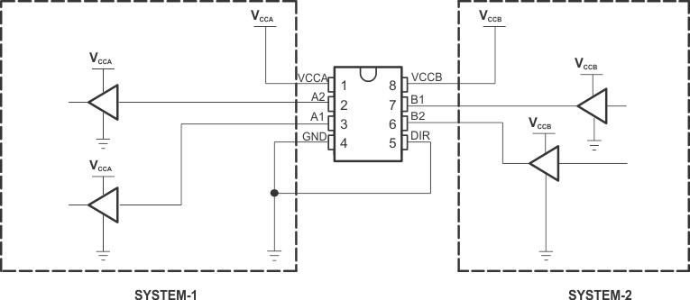
Figure 13 is an example circuit of the SN74AVC2T45 used in a unidirectional logic level-shifting application.
 Figure 13. Unidirectional Logic Level-Shifting Application
9.2.1.1 Design Requirements
Table 3 lists the pins and pin descriptions of the SN74AVC2T45 connections with SYSTEM-1 and SYSTEM-2.
Table 3. SN74AVC2T45 Pin Connections With SYSTEM-1 and SYSTEM-2
| PIN | NAME | DESCRIPTION |
|---|---|---|
| 1 | VCCA | SYSTEM-1 supply voltage (1.2 V to 3.6 V) |
| 2 | A1 | Output level depends on VCCA. |
| 3 | A2 | Output level depends on VCCA. |
| 4 | GND | Device GND |
| 5 | DIR | The GND (low-level) determines B-port to A-port direction. |
| 6 | B2 | Input threshold value depends on VCCB. |
| 7 | B1 | Input threshold value depends on VCCB. |
| 8 | VCCB | SYSTEM-2 supply voltage (1.2 V to 3.6 V) |
9.2.1.2 Detailed Design Procedure
This device uses drivers which are enabled depending on the state of the DIR pin. The designer must know the intended flow of data and take care not to violate any of the high or low logic levels. Unused data inputs must not be floating, as this can cause excessive internal leakage on the input CMOS structure. Make sure to tie any unused input and output ports directly to ground.
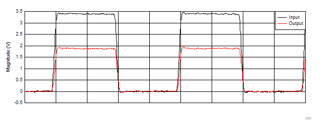
9.2.1.3 Application Curve
 Figure 14. 3.3 V to 1.8 V Level-Shifting With 1-MHz Square Wave
9.2.2 Bidirectional Logic Level-Shifting Application
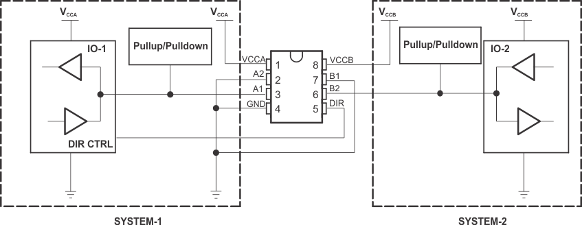
Figure 15 shows the SN74AVC2T45 used in a bidirectional logic level-shifting application.
 Figure 15. Bidirectional Logic Level-Shifting Application
9.2.2.1 Design Requirements
The SN74AVC2T45 does not have an output-enable (OE) pin, the system designer should take precautions to avoid bus contention between SYSTEM-1 and SYSTEM-2 when changing directions.
9.2.2.2 Detailed Design Procedure
Table 4 shows a sequence that illustrates data transmission from SYSTEM-1 to SYSTEM-2 and then from SYSTEM-2 to SYSTEM-1.
Table 4. Data Transmission Sequence
| STATE | DIR CTRL | IO-1 | IO-2 | DESCRIPTION |
|---|---|---|---|---|
| 1 | H | Output | Input | SYSTEM-1 data to SYSTEM-2 |
| 2 | H | Hi-Z | Hi-Z | SYSTEM-2 is getting ready to send data to SYSTEM-1. IO-1 and IO-2 are disabled. The bus-line state depends on pullup or pulldown.(1) |
| 3 | L | Hi-Z | Hi-Z | DIR bit is flipped. IO-1 and IO-2 still are disabled. The bus-line state depends on pullup or pulldown.(1) |
| 4 | L | Input | Output | SYSTEM-2 data to SYSTEM-1 |
9.2.2.2.1 Enable Times
Calculate the enable times for the SN74AVC2T45 using the following formulas:
- tPZH (DIR to A) = tPLZ (DIR to B) + tPLH (B to A)
- tPZL (DIR to A) = tPHZ (DIR to B) + tPHL (B to A)
- tPZH (DIR to B) = tPLZ (DIR to A) + tPLH (A to B)
- tPZL (DIR to B) = tPHZ (DIR to A) + tPHL (A to B)
In a bidirectional application, these enable times provide the maximum delay from the time the DIR bit is switched until an output is expected. For example, if the SN74AVC2T45 initially is transmitting from A to B, then the DIR bit is switched; the B port of the device must be disabled before presenting it with an input. After the B port has been disabled, an input signal applied to it appears on the corresponding A port after the specified propagation delay.