SCES531L December 2003 – May 2017 SN74AVC2T45
PRODUCTION DATA.
- 1 Features
- 2 Applications
- 3 Description
- 4 Revision History
- 5 Pin Configuration and Functions
-
6 Specifications
- 6.1 Absolute Maximum Ratings
- 6.2 ESD Ratings
- 6.3 Recommended Operating Conditions
- 6.4 Thermal Information
- 6.5 Electrical Characteristics
- 6.6 Switching Characteristics: VCCA = 1.2 V
- 6.7 Switching Characteristics: VCCA = 1.5 V ±0.1 V
- 6.8 Switching Characteristics: VCCA = 1.8 V ±0.15 V
- 6.9 Switching Characteristics: VCCA = 2.5 V ±0.2 V
- 6.10 Switching Characteristics: VCCA = 3.3 V ±0.3 V
- 6.11 Operating Characteristics
- 6.12
Typical Characteristics
- 6.12.1 Typical Propagation Delay (A to B) vs Load Capacitance, TA = 25°C, VCCA = 1.2 V
- 6.12.2 Typical Propagation Delay (A to B) vs Load Capacitance, TA = 25°C, VCCA = 1.5 V
- 6.12.3 Typical Propagation Delay (A-to-B) vs Load Capacitance, TA = 25°C, VCCA = 1.8 V
- 6.12.4 Typical Propagation Delay (A to B) vs Load Capacitance, TA = 25°C, VCCA = 2.5 V
- 6.12.5 Typical Propagation Delay (A to B) vs Load Capacitance, TA = 25°C, VCCA = 3.3 V
- 7 Parameter Measurement Information
- 8 Detailed Description
- 9 Application and Implementation
- 10Power Supply Recommendations
- 11Layout
- 12Device and Documentation Support
- 13Mechanical, Packaging, and Orderable Information
Package Options
Refer to the PDF data sheet for device specific package drawings
Mechanical Data (Package|Pins)
- DCU|8
- YZP|8
- DCT|8
Thermal pad, mechanical data (Package|Pins)
Orderable Information
8 Detailed Description
8.1 Overview
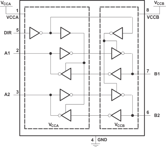
This dual-bit noninverting bus transceiver uses two separate configurable power-supply rails. The A port is designed to track VCCA and accepts any supply voltage from 1.2 V to 3.6 V. The B port is designed to track VCCB and accepts any supply voltage from 1.2 V to 3.6 V. This allows for universal low-voltage bidirectional translation and level-shifting between any of the 1.2 V, 1.5 V, 1.8 V, 2.5 V, and 3.3 V voltage nodes.
The SN74AVC2T45 is designed for asynchronous communication between two data buses. The logic levels of the direction-control (DIR) input activate either the B-port outputs or the A-port outputs. The device transmits data from the A bus to the B bus when the B-port outputs are activated and from the B bus to the A bus when the A-port outputs are activated. The input circuitry on both A and B ports always is active and must have a logic HIGH or LOW level applied to prevent excess internal leakage of the CMOS.
The SN74AVC2T45 is designed so that the DIR input is powered by supply voltage from VCCA.
This device is fully specified for partial-power-down applications using off output current (Ioff). The Ioff circuitry disables the outputs, preventing damaging current backflow through the device when it is powered down.
The VCC isolation feature ensures that if either VCC input is at GND, both ports are put in a high-impedance state. This will prevent a false high or low logic being presented at the output.
NanoFree package technology is a major breakthrough in IC packaging concepts, using the die as the package.
8.2 Functional Block Diagram
8.3 Feature Description
8.3.1 VCC Isolation
The VCC isolation feature ensures that if either VCCA or VCCB are at GND, both ports will be in a high-impedance state (IOZ shown in Electrical Characteristics). This prevents false logic levels from being presented to either bus.
8.3.2 2-Rail Design
Fully configurable 2-rail design allows each port to operate over the full 1.2 V to 3.6 V power-supply range.
8.3.3 IO Ports are 4.6-V Tolerant
The IO ports are up to 4.6 V tolerant.
8.3.4 Partial-Power-Down Mode
This device is fully specified for partial-power-down applications using off output current (Ioff). The Ioff circuitry disables the outputs, preventing damaging current backflow through the device when it is powered down.
