SCES531L December 2003 – May 2017 SN74AVC2T45
PRODUCTION DATA.
- 1 Features
- 2 Applications
- 3 Description
- 4 Revision History
- 5 Pin Configuration and Functions
-
6 Specifications
- 6.1 Absolute Maximum Ratings
- 6.2 ESD Ratings
- 6.3 Recommended Operating Conditions
- 6.4 Thermal Information
- 6.5 Electrical Characteristics
- 6.6 Switching Characteristics: VCCA = 1.2 V
- 6.7 Switching Characteristics: VCCA = 1.5 V ±0.1 V
- 6.8 Switching Characteristics: VCCA = 1.8 V ±0.15 V
- 6.9 Switching Characteristics: VCCA = 2.5 V ±0.2 V
- 6.10 Switching Characteristics: VCCA = 3.3 V ±0.3 V
- 6.11 Operating Characteristics
- 6.12
Typical Characteristics
- 6.12.1 Typical Propagation Delay (A to B) vs Load Capacitance, TA = 25°C, VCCA = 1.2 V
- 6.12.2 Typical Propagation Delay (A to B) vs Load Capacitance, TA = 25°C, VCCA = 1.5 V
- 6.12.3 Typical Propagation Delay (A-to-B) vs Load Capacitance, TA = 25°C, VCCA = 1.8 V
- 6.12.4 Typical Propagation Delay (A to B) vs Load Capacitance, TA = 25°C, VCCA = 2.5 V
- 6.12.5 Typical Propagation Delay (A to B) vs Load Capacitance, TA = 25°C, VCCA = 3.3 V
- 7 Parameter Measurement Information
- 8 Detailed Description
- 9 Application and Implementation
- 10Power Supply Recommendations
- 11Layout
- 12Device and Documentation Support
- 13Mechanical, Packaging, and Orderable Information
Package Options
Refer to the PDF data sheet for device specific package drawings
Mechanical Data (Package|Pins)
- DCU|8
- YZP|8
- DCT|8
Thermal pad, mechanical data (Package|Pins)
Orderable Information
6 Specifications
6.1 Absolute Maximum Ratings
over operating free-air temperature range (unless otherwise noted)(1)| MIN | MAX | UNIT | |||
|---|---|---|---|---|---|
| VCCA
VCCB |
Supply voltage | –0.5 | 4.6 | V | |
| VI | Input voltage(2) | IO ports (A port) | –0.5 | 4.6 | V |
| IO ports (B port) | –0.5 | 4.6 | |||
| Control inputs | –0.5 | 4.6 | |||
| VO | Voltage applied to any output in the high-impedance or power-off state(2) | A port | –0.5 | 4.6 | V |
| B port | –0.5 | 4.6 | |||
| VO | Voltage applied to any output in the high or low state(2) (3) | A port | –0.5 | VCCA + 0.5 | V |
| B port | –0.5 | VCCB + 0.5 | |||
| IIK | Input clamp current | VI < 0 | –50 | mA | |
| IOK | Output clamp current | VO < 0 | –50 | mA | |
| IO | Continuous output current | ±50 | mA | ||
| Continuous current through VCCA, VCCB, or GND | ±100 | mA | |||
| TJ | Junction temperature | 150 | °C | ||
| Tstg | Storage temperature | –65 | 150 | °C | |
(1) Stresses beyond those listed under Absolute Maximum Ratings may cause permanent damage to the device. These are stress ratings only, which do not imply functional operation of the device at these or any other conditions beyond those indicated under Recommended Operating Conditions. Exposure to absolute-maximum-rated conditions for extended periods may affect device reliability.
(2) The input negative-voltage and output voltage ratings may be exceeded if the input and output current ratings are observed.
(3) The output positive-voltage rating may be exceeded up to 4.6 V maximum if the output current ratings are observed.
6.2 ESD Ratings
| VALUE | UNIT | |||
|---|---|---|---|---|
| V(ESD) | Electrostatic discharge | Human body model (HBM), per ANSI/ESDA/JEDEC JS-001(1) | ±8000 | V |
| Charged-device model (CDM), per JEDEC specification JESD22-C101(2) | ±1000 | |||
| Machine Model (MM), Per JEDEC specification JESD22-A115-A | ±200 | |||
(1) JEDEC document JEP155 states that 500-V HBM allows safe manufacturing with a standard ESD control process.
(2) JEDEC document JEP157 states that 250-V CDM allows safe manufacturing with a standard ESD control process.
6.3 Recommended Operating Conditions
See(3)(4)(5)| VCCI (1) | VCCO (2) | MIN | MAX | UNIT | |||
|---|---|---|---|---|---|---|---|
| VCCA | Supply voltage | 1.2 | 3.6 | V | |||
| VCCB | Supply voltage | 1.2 | 3.6 | V | |||
| VIH | High-level input voltage |
Data inputs(4) | 1.2 V to 1.95 V | VCCI (1) × 0.65 | V | ||
| 1.95 V to 2.7 V | 1.6 | ||||||
| 2.7 V to 3.6 V | 2 | ||||||
| VIL | Low-level input voltage |
Data inputs(4) | 1.2 V to 1.95 V | VCCI (1) × 0.35 | V | ||
| 1.95 V to 2.7 V | 0.7 | ||||||
| 2.7 V to 3.6 V | 0.8 | ||||||
| VIH | High-level input voltage |
DIR (referenced to VCCA)(5) |
1.2 V to 1.95 V | VCCA × 0.65 | V | ||
| 1.95 V to 2.7 V | 1.6 | ||||||
| 2.7 V to 3.6 V | 2 | ||||||
| VIL | Low-level input voltage |
DIR (referenced to VCCA)(5) |
1.2 V to 1.95 V | VCCA × 0.35 | V | ||
| 1.95 V to 2.7 V | 0.7 | ||||||
| 2.7 V to 3.6 V | 0.8 | ||||||
| VI | Input voltage | 0 | 3.6 | V | |||
| VO | Output voltage | Active state | 0 | VCCO (2) | V | ||
| 3-state | 0 | 3.6 | |||||
| IOH | High-level output current | 1.2 V | –3 | mA | |||
| 1.4 V to 1.6 V | –6 | ||||||
| 1.65 V to 1.95 V | –8 | ||||||
| 2.3 V to 2.7 V | –9 | ||||||
| 3 V to 3.6 V | –12 | ||||||
| IOL | Low-level output current | 1.2 V | 3 | mA | |||
| 1.4 V to 1.6 V | 6 | ||||||
| 1.65 V to 1.95 V | 8 | ||||||
| 2.3 V to 2.7 V | 9 | ||||||
| 3 V to 3.6 V | 12 | ||||||
| Δt/Δv | Input transition rise or fall rate | 5 | ns/V | ||||
| TA | Operating free-air temperature | –40 | 85 | °C | |||
(1) VCCI is the voltage associated with the input port supply VCCA or VCCB.
(2) VCCO is the voltage associated with the output port supply VCCA or VCCB.
(3) All unused data inputs of the device must be held at VCCI or GND to ensure proper device operation. See Implications of Slow or Floating CMOS Inputs, SCBA004.
(4) For VCCI values not specified in the data sheet, VIH min = VCCI × 0.7 V, VIL max = VCCI × 0.3 V.
(5) For VCCI values not specified in the data sheet, VIH min = VCCA × 0.7 V, VIL max = VCCA × 0.3 V.
6.4 Thermal Information
| THERMAL METRIC(1) | SN74AVC2T45 | UNIT | |||
|---|---|---|---|---|---|
| DCT (SSOP) | DCU (VSSOP) | YZP (DSBGA) | |||
| 8 PINS | 8 PINS | 8 PINS | |||
| RθJA | Junction-to-ambient thermal resistance | 194.4 | 199.3 | 105.8 | °C/W |
| RθJC(top) | Junction-to-case (top) thermal resistance | 124.7 | 76.2 | 1.6 | °C/W |
| RθJB | Junction-to-board thermal resistance | 106.8 | 80.6 | 10.8 | °C/W |
| ψJT | Junction-to-top characterization parameter | 49.8 | 7.1 | 3.1 | °C/W |
| ψJB | Junction-to-board characterization parameter | 105.8 | 80.1 | 10.8 | °C/W |
(1) For more information about traditional and new thermal metrics, see the Semiconductor and IC Package Thermal Metrics application report.
6.5 Electrical Characteristics
over recommended operating free-air temperature range (unless otherwise noted)(1) (2)| PARAMETER | TEST CONDITIONS | VCCA | VCCB | TA = 25°C | –40°C to +85°C | UNIT | |||||
|---|---|---|---|---|---|---|---|---|---|---|---|
| MIN | TYP | MAX | MIN | MAX | |||||||
| VOH (3) | IOH = –100 µA | VI = VIH | 1.2 V to 3.6 V | 1.2 V to 3.6 V | VCCO – 0.2 V | V | |||||
| IOH = –3 mA | 1.2 V | 1.2 V | 0.95 | ||||||||
| IOH = –6 mA | 1.4 V | 1.4 V | 1.05 | ||||||||
| IOH = –8 mA | 1.65 V | 1.65 V | 1.2 | ||||||||
| IOH = –9 mA | 2.3 V | 2.3 V | 1.75 | ||||||||
| IOH = –12 mA | 3 V | 3 V | 2.3 | ||||||||
| VOL (3) | IOL = 100 µA | VI = VIL | 1.2 V to 3.6 V | 1.2 V to 3.6 V | 0.2 | V | |||||
| IOL = 3 mA | 1.2 V | 1.2 V | 0.25 | ||||||||
| IOL = 6 mA | 1.4 V | 1.4 V | 0.35 | ||||||||
| IOL = 8 mA | 1.65 V | 1.65 V | 0.45 | ||||||||
| IOL = 9 mA | 2.3 V | 2.3 V | 0.55 | ||||||||
| IOL = 12 mA | 3 V | 3 V | 0.7 | ||||||||
| II | DIR | VI = VCCA or GND | 1.2 V to 3.6 V | 1.2 V to 3.6 V | ±0.025 | ±0.25 | ±1 | µA | |||
| Ioff | A port | VI or VO = 0 to 3.6 V | 0 V | 0 to 3.6 V | ±0.1 | ±1 | ±5 | µA | |||
| B port | 0 to 3.6 V | 0 V | ±0.1 | ±1 | ±5 | ||||||
| IOZ (3) | B port | VO = VCCO or GND, VI = VCCI or GND |
0 V | 3.6 V | ±0.5 | ±2.5 | ±5 | µA | |||
| A port | 3.6 V | 0 V | ±0.5 | ±2.5 | ±5 | ||||||
| ICCA (3) | VI = VCCI or GND, IO = 0 | 1.2 V to 3.6 V | 1.2 V to 3.6 V | 10 | µA | ||||||
| 0 V | 3.6 V | –2 | |||||||||
| 3.6 V | 0 V | 10 | |||||||||
| ICCB (3) | VI = VCCI or GND, IO = 0 | 1.2 V to 3.6 V | 1.2 V to 3.6 V | 10 | µA | ||||||
| 0 V | 3.6 V | 10 | |||||||||
| 3.6 V | 0 V | –2 | |||||||||
| ICCA + ICCB
(see Table 1) |
VI = VCCI or GND, IO = 0 | 1.2 V to 3.6 V | 1.2 V to 3.6 V | 20 | µA | ||||||
| CI | Control inputs |
VI = 3.3 V or GND | 3.3 V | 3.3 V | 2.5 | pF | |||||
| Cio | A or B port |
VO = 3.3 V or GND | 3.3 V | 3.3 V | 6 | pF | |||||
(1) VCCO is the voltage associated with the output port supply VCCA or VCCB.
(2) VCCI is the voltage associated with the input port supply VCCA or VCCB.
(3) VOH: Output High Voltage; VOL: Output Low Voltage; IOZ: Hi-Z Output Current; ICCA: Supply A Current; ICCB: Supply B Current
6.6 Switching Characteristics: VCCA = 1.2 V
over recommended operating free-air temperature range, VCCA = 1.2 V (see Figure 11)| PARAMETER | FROM (INPUT) |
TO (OUTPUT) |
VCCB = 1.2 V | VCCB = 1.5 V | VCCB = 1.8 V | VCCB = 2.5 V | VCCB = 3.3 V | UNIT |
|---|---|---|---|---|---|---|---|---|
| TYP | TYP | TYP | TYP | TYP | ||||
| tPLH (2) | A | B | 3.1 | 2.6 | 2.4 | 2.2 | 2.2 | ns |
| tPHL (2) | 3.1 | 2.6 | 2.4 | 2.2 | 2.2 | |||
| tPLH (2) | B | A | 3.4 | 3.1 | 3 | 2.9 | 2.9 | ns |
| tPHL (2) | 3.4 | 3.1 | 3 | 2.9 | 2.9 | |||
| tPHZ (2) | DIR | A | 5.2 | 5.2 | 5.1 | 5 | 4.8 | ns |
| tPLZ (2) | 5.2 | 5.2 | 5.1 | 5 | 4.8 | |||
| tPHZ (2) | DIR | B | 5 | 4 | 3.8 | 2.8 | 3.2 | ns |
| tPLZ (2) | 5 | 4 | 3.8 | 2.8 | 3.2 | |||
| tPZH (2) (1) | DIR | A | 8.4 | 7.1 | 6.8 | 5.7 | 6.1 | ns |
| tPZL (2) (1) | 8.4 | 7.1 | 6.8 | 5.7 | 6.1 | |||
| tPZH (2) (1) | DIR | B | 8.3 | 7.8 | 7.5 | 7.2 | 7 | ns |
| tPZL (2) (1) | 8.3 | 7.8 | 7.5 | 7.2 | 7 |
(1) The enable time is a calculated value, derived using the formula shown in the Enable Times section.
(2) tPLH: Low-to-high Propagation Delay; tPHL: High-to-Low Propagation Delay; tPHZ: High-to-Hi-Z Propagation Delay; tPLZ: Low-to-Hi-Z Propagation Delay; tPZH: Hi-Z-to-High Propagation Delay; tPZL: Hi-Z-to-Low Propagation Delay
6.7 Switching Characteristics: VCCA = 1.5 V ±0.1 V
over recommended operating free-air temperature range, VCCA = 1.5 V ± 0.1 V (see Figure 11)| PARAMETER | FROM (INPUT) |
TO (OUTPUT) |
VCCB = 1.2 V | VCCB = 1.5 V ± 0.1 V |
VCCB = 1.8 V ± 0.15 V |
VCCB = 2.5 V ± 0.2 V |
VCCB = 3.3 V ± 0.3 V |
UNIT | ||||
|---|---|---|---|---|---|---|---|---|---|---|---|---|
| TYP | MIN | MAX | MIN | MAX | MIN | MAX | MIN | MAX | ||||
| tPLH (2) | A | B | 2.8 | 0.7 | 5.4 | 0.5 | 4.6 | 0.4 | 3.7 | 0.3 | 3.5 | ns |
| tPHL (2) | 2.8 | 0.7 | 5.4 | 0.5 | 4.6 | 0.4 | 3.7 | 0.3 | 3.5 | |||
| tPLH (2) | B | A | 2.7 | 0.8 | 5.4 | 0.7 | 5.2 | 0.6 | 4.9 | 0.5 | 4.7 | ns |
| tPHL (2) | 2.7 | 0.8 | 5.4 | 0.7 | 5.2 | 0.6 | 4.9 | 0.5 | 4.7 | |||
| tPHZ (2) | DIR | A | 3.9 | 1.3 | 8.5 | 1.3 | 7.8 | 1.1 | 7.7 | 1.4 | 7.6 | ns |
| tPLZ (2) | 3.9 | 1.3 | 8.5 | 1.3 | 7.8 | 1.1 | 7.7 | 1.4 | 7.6 | |||
| tPHZ (2) | DIR | B | 4.7 | 1.1 | 7 | 1.4 | 6.9 | 1.2 | 6.9 | 1.7 | 7.1 | ns |
| tPLZ (2) | 4.7 | 1.1 | 7 | 1.4 | 6.9 | 1.2 | 6.9 | 1.7 | 7.1 | |||
| tPZH (2) (1) | DIR | A | 7.4 | 12.4 | 12.1 | 11.8 | 11.8 | ns | ||||
| tPZL (2) (1) | 7.4 | 12.4 | 12.1 | 11.8 | 11.8 | |||||||
| tPZH (2) (1) | DIR | B | 6.7 | 13.9 | 12.4 | 11.4 | 11.1 | ns | ||||
| tPZL (2) (1) | 6.7 | 13.9 | 12.4 | 11.4 | 11.1 | |||||||
(1) The enable time is a calculated value, derived using the formula shown in the Enable Times section.
(2) tPLH: Low-to-high Propagation Delay; tPHL: High-to-Low Propagation Delay; tPHZ: High-to-Hi-Z Propagation Delay; tPLZ: Low-to-Hi-Z Propagation Delay; tPZH: Hi-Z-to-High Propagation Delay; tPZL: Hi-Z-to-Low Propagation Delay
6.8 Switching Characteristics: VCCA = 1.8 V ±0.15 V
over recommended operating free-air temperature range, VCCA = 1.8 V ± 0.15 V (see Figure 11)| PARAMETER | FROM (INPUT) |
TO (OUTPUT) |
VCCB = 1.2 V | VCCB = 1.5 V ± 0.1 V |
VCCB = 1.8 V ± 0.15 V |
VCCB = 2.5 V ± 0.2 V |
VCCB = 3.3 V ± 0.3 V |
UNIT | ||||
|---|---|---|---|---|---|---|---|---|---|---|---|---|
| TYP | MIN | MAX | MIN | MAX | MIN | MAX | MIN | MAX | ||||
| tPLH (2) | A | B | 2.7 | 0.5 | 5.2 | 0.4 | 4.3 | 0.2 | 3.4 | 0.2 | 3.1 | ns |
| tPHL (2) | 2.7 | 0.5 | 5.2 | 0.4 | 4.3 | 0.2 | 3.4 | 0.2 | 3.1 | |||
| tPLH (2) | B | A | 2.4 | 0.7 | 4.7 | 0.5 | 4.4 | 0.5 | 4 | 0.4 | 3.8 | ns |
| tPHL (2) | 2.4 | 0.7 | 4.7 | 0.5 | 4.4 | 0.5 | 4 | 0.4 | 3.8 | |||
| tPHZ (2) | DIR | A | 3.7 | 1.3 | 8.1 | 0.7 | 6.9 | 1.4 | 5.3 | 1.1 | 5.2 | ns |
| tPLZ (2) | 3.7 | 1.3 | 8.1 | 0.7 | 6.9 | 1.4 | 5.3 | 1.1 | 5.2 | |||
| tPHZ (2) | DIR | B | 4.4 | 1.3 | 5.8 | 1.3 | 5.9 | 0.8 | 5.7 | 1.5 | 5.9 | ns |
| tPLZ (2) | 4.4 | 1.3 | 5.8 | 1.3 | 5.9 | 0.8 | 5.7 | 1.5 | 5.9 | |||
| tPZH (2) (1) | DIR | A | 6.8 | 10.5 | 10.3 | 9.7 | 9.7 | ns | ||||
| tPZL (2) (1) | 6.8 | 10.5 | 10.3 | 9.7 | 9.7 | |||||||
| tPZH (2) (1) | DIR | B | 6.4 | 13.3 | 11.2 | 8.7 | 8.3 | ns | ||||
| tPZL (2) (1) | 6.4 | 13.3 | 11.2 | 8.7 | 8.3 | |||||||
(1) The enable time is a calculated value, derived using the formula shown in the Enable Times section.
(2) tPLH: Low-to-high Propagation Delay; tPHL: High-to-Low Propagation Delay; tPHZ: High-to-Hi-Z Propagation Delay; tPLZ: Low-to-Hi-Z Propagation Delay; tPZH: Hi-Z-to-High Propagation Delay; tPZL: Hi-Z-to-Low Propagation Delay
6.9 Switching Characteristics: VCCA = 2.5 V ±0.2 V
over recommended operating free-air temperature range, VCCA = 2.5 V ± 0.2 V (see Figure 11)| PARAMETER | FROM (INPUT) |
TO (OUTPUT) |
VCCB = 1.2 V | VCCB = 1.5 V ± 0.1 V |
VCCB = 1.8 V ± 0.15 V |
VCCB = 2.5 V ± 0.2 V |
VCCB = 3.3 V ± 0.3 V |
UNIT | ||||
|---|---|---|---|---|---|---|---|---|---|---|---|---|
| TYP | MIN | MAX | MIN | MAX | MIN | MAX | MIN | MAX | ||||
| tPLH (2) | A | B | 2.6 | 0.4 | 4.9 | 0.2 | 4 | 0.2 | 3 | 0.2 | 2.6 | ns |
| tPHL (2) | 2.6 | 0.4 | 4.9 | 0.2 | 4 | 0.2 | 3 | 0.2 | 2.6 | |||
| tPLH (2) | B | A | 2.1 | 0.6 | 3.8 | 0.5 | 3.4 | 0.4 | 3 | 0.3 | 2.8 | ns |
| tPHL (2) | 2.1 | 0.6 | 3.8 | 0.5 | 3.4 | 0.4 | 3 | 0.3 | 2.8 | |||
| tPHZ (2) | DIR | A | 2.4 | 0.7 | 7.9 | 0.8 | 6.4 | 0.8 | 5 | 0.5 | 4.3 | ns |
| tPLZ (2) | 2.4 | 0.7 | 7.9 | 0.8 | 6.4 | 0.8 | 5 | 0.5 | 4.3 | |||
| tPHZ (2) | DIR | B | 3.8 | 1 | 4.3 | 0.6 | 4.3 | 0.5 | 4.2 | 1.1 | 4.1 | ns |
| tPLZ (2) | 3.8 | 1 | 4.3 | 0.6 | 4.3 | 0.5 | 4.2 | 1.1 | 4.1 | |||
| tPZH (2) (1) | DIR | A | 5.9 | 8.5 | 7.7 | 7.2 | 6.9 | ns | ||||
| tPZL (2) (1) | 5.9 | 8.5 | 7.7 | 7.2 | 6.9 | |||||||
| tPZH (2) (1) | DIR | B | 5 | 12.8 | 10.4 | 8 | 6.9 | ns | ||||
| tPZL (2) (1) | 5 | 12.8 | 10.4 | 8 | 6.9 | |||||||
(1) The enable time is a calculated value, derived using the formula shown in the Enable Times section.
(2) tPLH: Low-to-high Propagation Delay; tPHL: High-to-Low Propagation Delay; tPHZ: High-to-Hi-Z Propagation Delay; tPLZ: Low-to-Hi-Z Propagation Delay; tPZH: Hi-Z-to-High Propagation Delay; tPZL: Hi-Z-to-Low Propagation Delay
6.10 Switching Characteristics: VCCA = 3.3 V ±0.3 V
over recommended operating free-air temperature range, VCCA = 3.3 V ± 0.3 V (see Figure 11)| PARAMETER | FROM (INPUT) |
TO (OUTPUT) |
VCCB = 1.2 V | VCCB = 1.5 V ± 0.1 V |
VCCB = 1.8 V ± 0.15 V |
VCCB = 2.5 V ± 0.2 V |
VCCB = 3.3 V ± 0.3 V |
UNIT | ||||
|---|---|---|---|---|---|---|---|---|---|---|---|---|
| TYP | MIN | MAX | MIN | MAX | MIN | MAX | MIN | MAX | ||||
| tPLH (2) | A | B | 2.5 | 0.3 | 4.7 | 0.2 | 3.8 | 0.2 | 2.8 | 0.2 | 2.4 | ns |
| tPHL (2) | 2.5 | 0.3 | 4.7 | 0.2 | 3.8 | 0.2 | 2.8 | 0.2 | 2.4 | |||
| tPLH (2) | B | A | 2.1 | 0.6 | 3.6 | 0.4 | 3.1 | 0.3 | 2.6 | 0.3 | 2.4 | ns |
| tPHL (2) | 2.1 | 0.6 | 3.6 | 0.4 | 3.1 | 0.3 | 2.6 | 0.3 | 2.4 | |||
| tPHZ (2) | DIR | A | 2.9 | 1.1 | 8 | 1 | 6.5 | 1.3 | 4.7 | 1.2 | 4 | ns |
| tPLZ (2) | 2.9 | 1.1 | 8 | 1 | 6.5 | 1.3 | 4.7 | 1.2 | 4 | |||
| tPHZ (2) | DIR | B | 3.4 | 0.5 | 6.6 | 0.3 | 5.6 | 0.3 | 4.6 | 1.1 | 4.2 | ns |
| tPLZ (2) | 3.4 | 0.5 | 6.6 | 0.3 | 5.6 | 0.3 | 4.6 | 1.1 | 4.2 | |||
| tPZH (2) (1) | DIR | A | 5.5 | 10.2 | 8.7 | 7.2 | 6.6 | ns | ||||
| tPZL (2) (1) | 5.5 | 10.2 | 8.7 | 7.2 | 6.6 | |||||||
| tPZH (2) (1) | DIR | B | 5.4 | 12.7 | 10.3 | 7.5 | 6.4 | ns | ||||
| tPZL (2) (1) | 5.4 | 12.7 | 10.3 | 7.5 | 6.4 | |||||||
(1) The enable time is a calculated value, derived using the formula shown in the section.
(2) tPLH: Low-to-high Propagation Delay; tPHL: High-to-Low Propagation Delay; tPHZ: High-to-Hi-Z Propagation Delay; tPLZ: Low-to-Hi-Z Propagation Delay; tPZH: Hi-Z-to-High Propagation Delay; tPZL: Hi-Z-to-Low Propagation Delay
6.11 Operating Characteristics
TA = 25°C| PARAMETER | TEST CONDITIONS |
VCCA = VCCB = 1.2 V |
VCCA = VCCB = 1.5 V |
VCCA = VCCB = 1.8 V |
VCCA = VCCB = 2.5 V |
VCCA = VCCB = 3.3 V |
UNIT | |
|---|---|---|---|---|---|---|---|---|
| TYP | TYP | TYP | TYP | TYP | ||||
| CpdA (1) | A-port input, B-port output |
CL = 0, f = 10 MHz, tr (2) = tf (2) = 1 ns |
3 | 3 | 3 | 3 | 4 | pF |
| B-port input, A-port output |
12 | 13 | 13 | 14 | 15 | |||
| CpdB (1) | A-port input, B-port output |
CL = 0, f = 10 MHz, tr (2) = tf (2) = 1 ns |
12 | 13 | 13 | 14 | 15 | pF |
| B-port input, A-port output |
3 | 3 | 3 | 3 | 4 | |||
(1) Power-dissipation capacitance per transceiver
(2) tr: Rise time; tf: Fall time
6.12 Typical Characteristics
Table 1. Typical Total Static Power Consumption (ICCA + ICCB)
| VCCB | VCCA | UNIT | |||||
|---|---|---|---|---|---|---|---|
| 0 V | 1.2 V | 1.5 V | 1.8 V | 2.5 V | 3.3 V | ||
| 0 V | 0 | <0.5 | <0.5 | <0.5 | <0.5 | <0.5 | µA |
| 1.2 V | <0.5 | <1 | <1 | <1 | <1 | 1 | |
| 1.5 V | <0.5 | <1 | <1 | <1 | <1 | 1 | |
| 1.8 V | <0.5 | <1 | <1 | <1 | <1 | <1 | |
| 2.5 V | <0.5 | 1 | <1 | <1 | <1 | <1 | |
| 3.3 V | <0.5 | 1 | <1 | <1 | <1 | <1 | |
6.12.1 Typical Propagation Delay (A to B) vs Load Capacitance, TA = 25°C, VCCA = 1.2 V
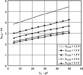 Figure 1. Typical A-to-B Propagation Delay, Low to High
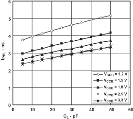 Figure 2. Typical A-to-B Propagation Delay, High to Low
6.12.2 Typical Propagation Delay (A to B) vs Load Capacitance, TA = 25°C, VCCA = 1.5 V
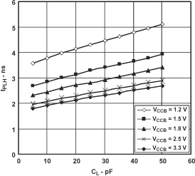 Figure 3. Typical A-to-B Propagation Delay, Low to High
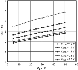 Figure 4. Typical A-to-B Propagation Delay, High to Low
6.12.3 Typical Propagation Delay (A-to-B) vs Load Capacitance, TA = 25°C, VCCA = 1.8 V
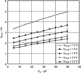 Figure 5. Typical A-to-B Propagation Delay, Low to High
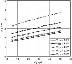 Figure 6. Typical A-to-B Propagation Delay, High to Low
6.12.4 Typical Propagation Delay (A to B) vs Load Capacitance, TA = 25°C, VCCA = 2.5 V
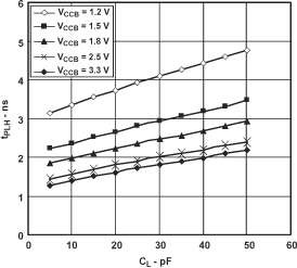 Figure 7. Typical A-to-B Propagation Delay, Low to High
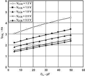 Figure 8. Typical A-to-B Propagation Delay, High to Low
6.12.5 Typical Propagation Delay (A to B) vs Load Capacitance, TA = 25°C, VCCA = 3.3 V
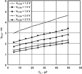 Figure 9. Typical A-to-B Propagation Delay, Low to High
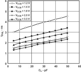 Figure 10. Typical A-to-B Propagation Delay, High to Low