SCES553H May 2004 – November 2020 SN74AVC32T245
PRODUCTION DATA
- 1 Features
- 2 Applications
- 3 Description
- 4 Revison History
- 5 Description (continued)
- 6 Pin Configuration and Functions
-
7 Specifications
- 7.1 Absolute Maximum Ratings
- 7.2 ESD Ratings
- 7.3 Thermal Information
- 7.4 Recommended Operating Conditions
- 7.5 Electrical Characteristics
- 7.6 Switching Characteristics: VCCA = 1.2 V
- 7.7 Switching Characteristics: VCCA = 1.5 V ± 0.1 V
- 7.8 Switching Characteristics: VCCA = 1.8 V ± 0.15 V
- 7.9 Switching Characteristics: VCCA = 2.5 V ± 0.2 V
- 7.10 Switching Characteristics: VCCA = 3.3 V ± 0.3 V
- 7.11 Operating Characteristics
- 7.12 Typical Characteristics
- 8 Parameter Measurement Information
- 9 Detailed Description
- 10Application and Implementation
- 11Power Supply Recommendations
- 12Layout
- 13Device and Documentation Support
- 14Mechanical, Packaging, and Orderable Information
Package Options
Mechanical Data (Package|Pins)
- NMJ|96
Thermal pad, mechanical data (Package|Pins)
Orderable Information
3 Description
This 32-bit noninverting bus transceiver uses two separate, configurable power-supply rails. The SN74AVC32T245 device is optimized to operate with VCCA/VCCB set from 1.4 V to 3.6 V. It is operational with VCCA/VCCB as low as 1.2 V. The A port is designed to track VCCA. VCCA and accepts any supply voltage from 1.2 V to 3.6 V. The B port is designed to track VCCB. VCCB and accepts any supply voltage from 1.2 V to 3.6 V. This allows for universal low-voltage bidirectional translation between any of the 1.2 V, 1.5 V, 1.8 V, 2.5 V, and 3.3 V voltage nodes.
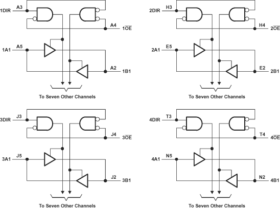
The SN74AVC32T245 is designed for asynchronous communication between data buses. The device transmits data from the A bus to the B bus or from the B bus to the A bus, depending on the logic level at the direction-control (DIR) input. The output-enable ( OE) input can disable the outputs so the buses are effectively isolated.
The SN74AVC32T245 is designed so that the control pins (1DIR, 2DIR, 3DIR, 4DIR, 1 OE, 2 OE, 3 OE, and 4 OE) are supplied by VCCA.
| PART NUMBER | PACKAGE(1) | BODY SIZE (NOM) |
|---|---|---|
| SN74AVC32T245ZKE/GKE | LFBGA (96) | 13.50 mm × 5.50 mm |
| SN74AVC32T245ZRL | BGA MICROSTAR JUNIOR (96) | 8.50 mm × 3.50 mm |
| SN74AVC32T245NMJ | nFBGA (96) | 13.50 mm × 5.50 mm |
 Figure 3-1 Logic Diagram