SCES693H February 2008 – March 2024 SN74AVC4T774
PRODUCTION DATA
- 1
- 1 Features
- 2 Applications
- 3 Description
- 4 Pin Configuration and Functions
-
5 Specifications
- 5.1 Absolute Maximum Ratings
- 5.2 ESD Ratings
- 5.3 Recommended Operating Conditions
- 5.4 Thermal Information
- 5.5 Electrical Characteristics
- 5.6 Switching Characteristics: VCCA = 1.2 V ± 0.1 V
- 5.7 Switching Characteristics: VCCA = 1.5 V ± 0.1 V
- 5.8 Switching Characteristics: VCCA = 1.8 V ± 0.15 V
- 5.9 Switching Characteristics: VCCA = 2.5 V ± 0.2 V
- 5.10 Switching Characteristics: VCCA = 3.3 V ± 0.3 V
- 5.11 Typical Characteristics
- 6 Parameter Measurement Information
- 7 Detailed Description
- 8 Application and Implementation
- 9 Device and Documentation Support
- 10Revision History
- 11Mechanical, Packaging, and Orderable Information
Package Options
Mechanical Data (Package|Pins)
Thermal pad, mechanical data (Package|Pins)
- RGY|16
Orderable Information
6.1 Load Circuit and Voltage Waveforms
Unless otherwise noted, all input pulses are supplied by generators having the following characteristics:
- f = 10 MHz
- ZO = 50 Ω
- Δt/ΔV ≤ 1 ns/V

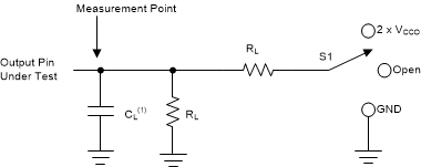
A. CL includes probe and
jig capacitance.
Figure 6-1 Load CircuitTable 6-1 Load Circuit
Parameters
| Test Parameter | S1 | |
|---|---|---|
| tpd | Propagation (delay) time | Open |
| tPZL, tPLZ | Enable time, disable time | 2 × VCCO |
| tPZH, tPHZ | Enable time, disable time | GND |
Table 6-2 Load Circuit Conditions
| VCCO | RL | CL | VTP |
|---|---|---|---|
| 1.2 V ± 0.1 V | 2 kΩ | 15 pF | 0.1 V |
| 1.5 V ± 0.1 V | 2 kΩ | 15 pF | 0.1 V |
| 1.8 V ± 0.15 V | 2 kΩ | 15 pF | 0.15 V |
| 2.5 V ± 0.2 V | 2 kΩ | 15 pF | 0.15 V |
| 3.3 V ± 0.3 V | 2 kΩ | 15 pF | 0.3 V |

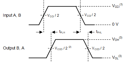
- VCCI is the VCC associated with the input port.
- VCCO is the VCC associated with the output port.
- VOH and VOL are typical output voltage levels that occur with specified RL, CL, and S1.
- tPLH and tPHL are the same as tpd.
- The outputs are measured one at a time, with one transition per measurement.

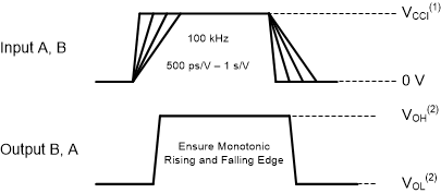
- VCCI is the supply pin associated with the input port.
- VOH and VOL are typical output voltage levels that occur with specified RL, CL, and S1.

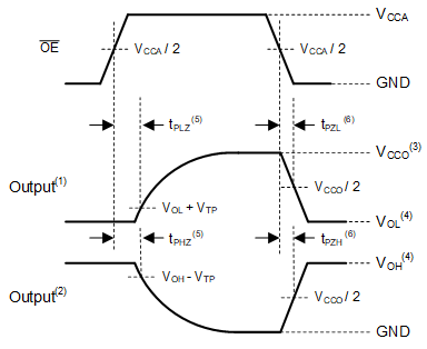
A. Output waveform on the condition
that input is driven to a valid Logic Low.
B. Output waveform on the condition
that input is driven to a valid Logic High.
C. VCCO is the supply pin
associated with the output port.
D. VOH and VOL
are typical output voltage levels with specified RL, CL,
and S1.
E. tPLZ and
tPHZ are the same as tdis.
F. tPZL and
tPZH are the same as ten.
Figure 6-4 Enable
Time And Disable Time