SCES577E JUNE 2004 – November 2015 SN74AVCH4T245
PRODUCTION DATA.
- 1 Features
- 2 Applications
- 3 Description
- 4 Revision History
- 5 Description (continued)
- 6 Pin Configuration and Functions
-
7 Specifications
- 7.1 Absolute Maximum Ratings
- 7.2 ESD Ratings
- 7.3 Recommended Operating Conditions
- 7.4 Thermal Information
- 7.5 Electrical Characteristics
- 7.6 Switching Characteristics, VCCA = 1.2 V
- 7.7 Switching Characteristics, VCCA = 1.5 V ± 0.1 V
- 7.8 Switching Characteristics, VCCA = 1.8 V ± 0.15 V
- 7.9 Switching Characteristics, VCCA = 2.5 V ± 0.2 V
- 7.10 Switching Characteristics, VCCA = 3.3 V ± 0.3 V
- 7.11 Operating Characteristics
- 7.12 Typical Characteristics
- 8 Parameter Measurement Information
- 9 Detailed Description
- 10Application and Implementation
- 11Power Supply Recommendations
- 12Layout
- 13Device and Documentation Support
- 14Mechanical, Packaging, and Orderable Information
Package Options
Mechanical Data (Package|Pins)
Thermal pad, mechanical data (Package|Pins)
- RGY|16
Orderable Information
1 Features
- Control Inputs VIH/VIL Levels are Referenced to VCCA Voltage
- Fully Configurable Dual-Rail Design Allows Each Port to Operate Over the Full 1.2V to 3.6V Power-Supply Range
- I/Os Are 4.6V Tolerant
- Ioff Supports Partial Power-Down-Mode Operation
- Bus Hold on Data Inputs Eliminates the Need for External pull-up/pull-down Resistors
- Max Data Rates
- 380 Mbps (1.8 V to 3.3 V Translation)
- 200 Mbps (<1.8 V to 3.3 V Translation)
- 200 Mbps (Translate to 2.5 V or 1.8 V)
- 150 Mbps (Translate to 1.5 V)
- 100 Mbps (Translate to 1.2 V)
- Latch-Up Performance Exceeds 100 mA Per JESD 78, Class II
- ESD Protection Exceeds JESD 22
- 8000 V Human Body Model (A114-A)
- 200 V Machine Model (A115-A)
- 1000 V Charged-Device Model (C101)
2 Applications
- Personal Electronics
- Industrial
- Enterprise
- Telecom
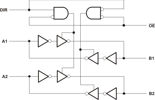
Logic Diagram (Positive Logic) for 1/2 of AVCH4T245

3 Description
This 4-bit noninverting bus transceiver uses two separate configurable power-supply rails. The A port is designed to track VCCA. VCCA accepts any supply voltage from 1.2 V to 3.6 V. The B port is designed to track VCCB. VCCB accepts any supply voltage from 1.2 V to 3.6 V. The SN74AVCH4T245 is optimized to operate with VCCA/VCCB set at 1.4 V to 3.6 V. It is operational with VCCA/VCCB as low as 1.2 V. This allows for universal low voltage bidirectional translation between any of the 1.2V, 1.5V, 1.8V, 2.5V, and 3.3V voltage nodes.
The SN74AVCH4T245 is designed for asynchronous communication between two data buses. The logic levels of the direction-control (DIR) input and the output-enable (OE) input activate either the B-port outputs or the A-port outputs or place both output ports into the high-impedance mode. The device transmits data from the A bus to the B bus when the B-port outputs are activated, and from the B bus to the A bus when the A-port outputs are activated. The input circuitry on both A and B ports is always active and must have a logic HIGH or LOW level applied to prevent excess ICC and ICCZ.
The SN74AVCH4T245 device control pins (1DIR, 2DIR, 1OE, and 2OE) are supplied by VCCA.
This device is fully specified for partial-power-down applications using Ioff. The Ioff circuitry disables the outputs, preventing damaging current backflow through the device when it is powered down.
Device Information(1)
| PART NUMBER | PACKAGE | BODY SIZE (NOM) |
|---|---|---|
| SN74AVCH4T245 | UQFN (16) | 1.80 mm × 2.60 mm |
| VQFN (16) | 3.50 mm × 4.00 mm | |
| TVSOP (16) | 4.40 mm × 3.60 mm | |
| TSSOP (16) | 4.40 mm × 5.00 mm | |
| SOIC (16) | 3.91 mm × 9.90 mm |
- For all available packages, see the orderable addendum at the end of the data sheet.
4 Revision History
Changes from D Revision (June 2007) to E Revision
- Added ESD Ratings table, Feature Description section, Device Functional Modes, Application and Implementation section, Power Supply Recommendations section, Layout section, Device and Documentation Support section, and Mechanical, Packaging, and Orderable Information sectionGo
- Changed Pin Functions table. Go