SCES577E JUNE 2004 – November 2015 SN74AVCH4T245
PRODUCTION DATA.
- 1 Features
- 2 Applications
- 3 Description
- 4 Revision History
- 5 Description (continued)
- 6 Pin Configuration and Functions
-
7 Specifications
- 7.1 Absolute Maximum Ratings
- 7.2 ESD Ratings
- 7.3 Recommended Operating Conditions
- 7.4 Thermal Information
- 7.5 Electrical Characteristics
- 7.6 Switching Characteristics, VCCA = 1.2 V
- 7.7 Switching Characteristics, VCCA = 1.5 V ± 0.1 V
- 7.8 Switching Characteristics, VCCA = 1.8 V ± 0.15 V
- 7.9 Switching Characteristics, VCCA = 2.5 V ± 0.2 V
- 7.10 Switching Characteristics, VCCA = 3.3 V ± 0.3 V
- 7.11 Operating Characteristics
- 7.12 Typical Characteristics
- 8 Parameter Measurement Information
- 9 Detailed Description
- 10Application and Implementation
- 11Power Supply Recommendations
- 12Layout
- 13Device and Documentation Support
- 14Mechanical, Packaging, and Orderable Information
Package Options
Mechanical Data (Package|Pins)
Thermal pad, mechanical data (Package|Pins)
- RGY|16
Orderable Information
10 Application and Implementation
NOTE
Information in the following applications sections is not part of the TI component specification, and TI does not warrant its accuracy or completeness. TI’s customers are responsible for determining suitability of components for their purposes. Customers should validate and test their design implementation to confirm system functionality.
10.1 Application Information
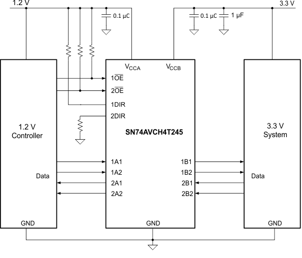
The SN74AVCH4T245 device can be used in level-shifting applications for interfacing devices or systems operating at different interface voltages with one another. The SN74AVCH4T245 device is ideal for use in applications where a push-pull driver is connected to the data I/Os. The max data rate can be up to 380 Mbps when device translates a signal from 1.8 V to 3.3 V.
10.2 Typical Application
10.2.1 Design Requirements
For the design example shown in Typical Application, use the parameters listed in Table 2.
Table 2. Design Parameters
| DESIGN PARAMETER | EXAMPLE VALUE |
|---|---|
| Input voltage range | 1.2 V to 3.6 V |
| Output voltage range | 1.2 V to 3.6 V |
10.2.2 Detailed Design Procedure
To begin the design process, determine the following:
- Input voltage range
- Use the supply voltage of the device that is driving the SN74AVCH4T245 device to determine the input voltage range. For a valid logic high, the value must exceed the VIH of the input port. For a valid logic low, the value must be less than the VIL of the input port.
- Output voltage range
- Use the supply voltage of the device that the SN74AVCH4T245 device is driving to determine the output voltage range.
10.2.3 Application Curve
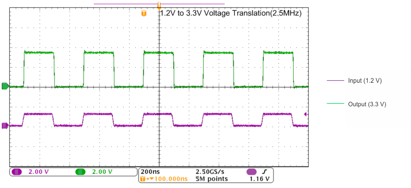
 Figure 6. Translation Up (1.2 V to 3.3 V) at 2.5 MHz
