SCES577E JUNE 2004 – November 2015 SN74AVCH4T245
PRODUCTION DATA.
- 1 Features
- 2 Applications
- 3 Description
- 4 Revision History
- 5 Description (continued)
- 6 Pin Configuration and Functions
-
7 Specifications
- 7.1 Absolute Maximum Ratings
- 7.2 ESD Ratings
- 7.3 Recommended Operating Conditions
- 7.4 Thermal Information
- 7.5 Electrical Characteristics
- 7.6 Switching Characteristics, VCCA = 1.2 V
- 7.7 Switching Characteristics, VCCA = 1.5 V ± 0.1 V
- 7.8 Switching Characteristics, VCCA = 1.8 V ± 0.15 V
- 7.9 Switching Characteristics, VCCA = 2.5 V ± 0.2 V
- 7.10 Switching Characteristics, VCCA = 3.3 V ± 0.3 V
- 7.11 Operating Characteristics
- 7.12 Typical Characteristics
- 8 Parameter Measurement Information
- 9 Detailed Description
- 10Application and Implementation
- 11Power Supply Recommendations
- 12Layout
- 13Device and Documentation Support
- 14Mechanical, Packaging, and Orderable Information
Package Options
Mechanical Data (Package|Pins)
Thermal pad, mechanical data (Package|Pins)
- RGY|16
Orderable Information
9 Detailed Description
9.1 Overview
The SN74AVCH4T245 is a 4-bit, dual-supply noninverting bidirectional voltage level translation device. Ax pins and control pins (1DIR, 2DIR,1OE, and 2OE) are supported by VCCA, and Bx pins are supported by VCCB. The A port is able to accept I/O voltages ranging from 1.2 V to 3.6 V, while the B port can accept I/O voltages from 1.2 V to 3.6 V. A high on DIR allows data transmission from Ax to Bx and a low on DIR allows data transmission from Bx to Ax when OE is set to low. When OE is set to high, both Ax and Bx pins are in the high-impedance state. Refer to the AVC Logic Family Technology and Applications Application Report SCEA006).
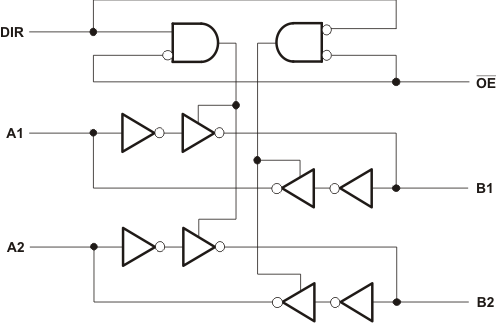
9.2 Functional Block Diagram
 Figure 4. Logic Diagram (Positive Logic) for 1/2 of SN74AVCH4T245
9.3 Feature Description
9.3.1 Fully Configurable Dual-Rail Design Allows Each Port to Operate Over the Full 1.2V to 3.6V Power-Supply Range
Both VCCA and VCCB can be supplied at any voltage between 1.2 V and 3.6 V; thus, making the device suitable for translating between any of the low voltage nodes (1.2 V, 1.8 V, 2.5 V, and 3.3 V).
9.3.2 Supports High Speed Translation
The SN74AVCH4T245 device can support high data rate applications. The translated signal data rate can be up to 380 Mbps when the signal is translated from 1.8 V to 3.3 V.
9.3.3 Ioff Supports Partial-Power-Down Mode Operation
Ioff will prevent backflow current by disabling I/O output circuits when device is in partial-power-down mode.
9.3.4 Bus-Hold Circuitry
This device has active bus-hold circuitry that holds unused or undriven inputs at a valid logic state. Use of pull-up or pull-down resistors with the bus-hold circuitry is not recommended. (Refer to the Bus-Hold Circuit Application Report (SCLA015). Pullup and pulldown resistors are not recommended on the inputs of devices with bus-hold. Unused inputs can be left floating.
9.3.5 Vcc Isolation Feature
The VCC isolation feature ensures that if either VCCA or VCCB are at GND (or < 0.4V), both ports will be in a high-impedance state (IOZ shown in Electrical Characteristics). This prevents false logic levels from being presented to either bus.
9.4 Device Functional Modes
Table 1 lists the functional modes of the SN74AVCH4T245.
Table 1. Function Table (Each 2-Bit Section)
| CONTROL INPUTS(1) | OUTPUT CIRCUITS | OPERATION | ||
|---|---|---|---|---|
| OE | DIR | A PORT | B PORT | |
| L | L | Enabled | Hi-Z | B data to A bus |
| L | H | Hi-Z | Enabled | A data to B bus |
| H | X | Hi-Z | Hi-Z | Isolation |