SCES882E December 2017 – December 2023 SN74AXC1T45
PRODUCTION DATA
- 1
- 1 Features
- 2 Applications
- 3 Description
- 4 Pin Configuration and Functions
- 5 Specifications
- 6 Parameter Measurement Information
- 7 Detailed Description
- 8 Application and Implementation
- 9 Device and Documentation Support
- 10Revision History
- 11Mechanical, Packaging, and Orderable Information
Package Options
Mechanical Data (Package|Pins)
Thermal pad, mechanical data (Package|Pins)
- DCK|6
Orderable Information
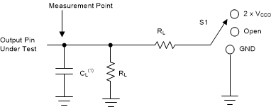
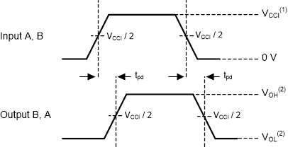
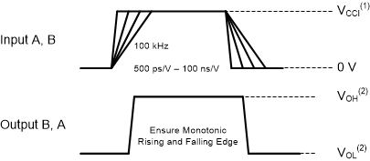
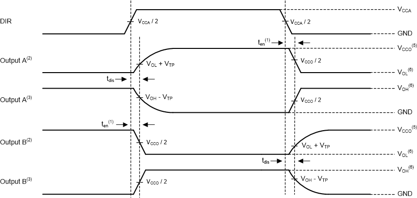
6.1 Load Circuit and Voltage Waveforms
Unless otherwise noted, all input pulses are supplied by generators having the following characteristics:
- f = 1 MHz
- ZO = 50 Ω
- dv/dt ≤ 1 ns/V

A. CL includes probe and jig capacitance.
Figure 6-1 Load CircuitTable 6-1 Load Circuit Conditions
| Parameter | VCCO | RL | CL | S1 | VTP | |
|---|---|---|---|---|---|---|
| Δt/Δv | Input transition rise or fall rate | 0.65 V – 3.6V | 1MΩ | 15pF | Open | N/A |
| tpd | Propagation (delay) time | 1.1V – 3.6V | 2kΩ | 15pF | Open | N/A |
| 0.65 V – 0.95 V | 20kΩ | 15pF | Open | N/A | ||
| ten, tdis | Enable time, disable time | 3V – 3.6V | 2kΩ | 15pF | 2 × VCCO | 0.3V |
| 1.65 V – 2.7V | 2kΩ | 15pF | 2 × VCCO | 0.15 V | ||
| 1.1V – 1.6V | 2kΩ | 15pF | 2 × VCCO | 0.1V | ||
| 0.65 V – 0.95 V | 20kΩ | 15pF | 2 × VCCO | 0.1V | ||
| ten, tdis | Enable time, disable time | 3V – 3.6V | 2kΩ | 15pF | GND | 0.3V |
| 1.65 V – 2.7V | 2kΩ | 15pF | GND | 0.15 V | ||
| 1.1V – 1.6V | 2kΩ | 15pF | GND | 0.1V | ||
| 0.65 V – 0.95 V | 20kΩ | 15pF | GND | 0.1V | ||

- VCCI is the supply pin associated with the input port.
- VOH and VOL are typical output voltage levels that occur with specified RL, CL, and S1

- VCCI is the supply pin associated with the input port.
- VOH and VOL are typical output voltage levels that occur with specified RL, CL, and S1

- Illustrative purposes only. Enable Time is a calculation as described in the data sheet.
- Output waveform on the condition that input is driven to a valid Logic Low.
- Output waveform on the condition that input is driven to a valid Logic High.
- VCCI is the supply pin associated with the input port
- VCCO is the supply pin associated with the output port.
- VOH and VOL are typical output voltage levels that occur with specified RL, CL, and S1