SCES908A February 2020 – April 2020 SN74AXC2T245-Q1
PRODUCTION DATA.
- 1 Features
- 2 Applications
- 3 Description
- 4 Revision History
- 5 Pin Configuration and Functions
-
6 Specifications
- 6.1 Absolute Maximum Ratings
- 6.2 ESD Ratings
- 6.3 Recommended Operating Conditions
- 6.4 Thermal Information
- 6.5 Electrical Characteristics
- 6.6 Switching Characteristics, VCCA = 0.7 ± 0.05 V
- 6.7 Switching Characteristics, VCCA = 0.8 ± 0.04 V
- 6.8 Switching Characteristics, VCCA = 0.9 ± 0.045 V
- 6.9 Switching Characteristics, VCCA = 1.2 ± 0.1 V
- 6.10 Switching Characteristics, VCCA = 1.5 ± 0.1 V
- 6.11 Switching Characteristics, VCCA = 1.8 ± 0.15 V
- 6.12 Switching Characteristics, VCCA = 2.5 ± 0.2 V
- 6.13 Switching Characteristics, VCCA = 3.3 ± 0.3 V
- 6.14 Operating Characteristics: TA = 25°C
- 7 Parameter Measurement Information
-
8 Detailed Description
- 8.1 Overview
- 8.2 Functional Block Diagram
- 8.3
Feature Description
- 8.3.1 Standard CMOS Inputs
- 8.3.2 Balanced High-Drive CMOS Push-Pull Outputs
- 8.3.3 Partial Power Down (Ioff)
- 8.3.4 VCC Isolation
- 8.3.5 Over-voltage Tolerant Inputs
- 8.3.6 Glitch-free Power Supply Sequencing
- 8.3.7 Negative Clamping Diodes
- 8.3.8 Fully Configurable Dual-Rail Design
- 8.3.9 Supports High-Speed Translation
- 8.4 Device Functional Modes
- 9 Application and Implementation
- 10Power Supply Recommendations
- 11Layout
- 12Device and Documentation Support
- 13Mechanical, Packaging, and Orderable Information
Package Options
Mechanical Data (Package|Pins)
- RSW|10
Thermal pad, mechanical data (Package|Pins)
Orderable Information
7.1 Load Circuit and Voltage Waveforms
Unless otherwise noted, all input pulses are supplied by generators having the following characteristics:
- f = 1 MHz
- ZO = 50 Ω
- dv/dt ≤ 1 ns/V

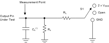
1. CL includes probe and jig capacitance.
Figure 1. Load Circuit Table 1. Load Circuit Conditions
| Parameter | VCCO | RL | CL | S1 | VTP | |
|---|---|---|---|---|---|---|
| Δt/Δv | Input transition rise or fall rate | 0.65 V – 3.6 V | 1 MΩ | 15 pF | Open | N/A |
| tpd | Propagation (delay) time | 1.1 V – 3.6 V | 2 kΩ | 15 pF | Open | N/A |
| 0.65 V – 0.95 V | 20 kΩ | 15 pF | Open | N/A | ||
| ten, tdis | Enable time, disable time | 3 V – 3.6 V | 2 kΩ | 15 pF | 2 × VCCO | 0.3 V |
| 1.65 V – 2.7 V | 2 kΩ | 15 pF | 2 × VCCO | 0.15 V | ||
| 1.1 V – 1.6 V | 2 kΩ | 15 pF | 2 × VCCO | 0.1 V | ||
| 0.65 V – 0.95 V | 20 kΩ | 15 pF | 2 × VCCO | 0.1 V | ||
| ten, tdis | Enable time, disable time | 3 V – 3.6 V | 2 kΩ | 15 pF | GND | 0.3 V |
| 1.65 V – 2.7 V | 2 kΩ | 15 pF | GND | 0.15 V | ||
| 1.1 V – 1.6 V | 2 kΩ | 15 pF | GND | 0.1 V | ||
| 0.65 V – 0.95 V | 20 kΩ | 15 pF | GND | 0.1 V | ||

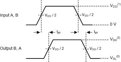
- VCCI is the supply pin associated with the input port.
- VOH and VOL are typical output voltage levels that occur with specified RL, CL, and S1

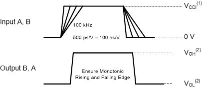
- VCCI is the supply pin associated with the input port.
- VOH and VOL are typical output voltage levels that occur with specified RL, CL, and S1

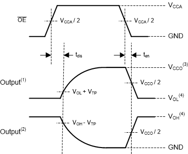
1. Output waveform on the condition that input is driven to a valid Logic Low.
2. Output waveform on the condition that input is driven to a valid Logic High.
3. VCCO is the supply pin associated with the output port.
4. VOH and VOL are typical output voltage levels with specified RL, CL, and S1.
Figure 4. Enable Time And Disable Time