SCES883C December 2018 – September 2020 SN74AXCH1T45
PRODUCTION DATA
- 1 Features
- 2 Applications
- 3 Description
- 4 Revision History
- 5 Pin Configuration and Functions
-
6 Specifications
- 6.1 Absolute Maximum Ratings
- 6.2 ESD Ratings
- 6.3 Recommended Operating Conditions
- 6.4 Thermal Information
- 6.5 Electrical Characteristics
- 6.6 Switching Characteristics, VCCA = 0.7 V
- 6.7 Switching Characteristics, VCCA = 0.8 V
- 6.8 Switching Characteristics, VCCA = 0.9 V
- 6.9 Switching Characteristics, VCCA = 1.2 V
- 6.10 Switching Characteristics, VCCA = 1.5 V
- 6.11 Switching Characteristics, VCCA = 1.8 V
- 6.12 Switching Characteristics, VCCA = 2.5 V
- 6.13 Switching Characteristics, VCCA = 3.3 V
- 6.14 Operating Characteristics: TA = 25°C
- 6.15 Typical Characteristics
- 7 Parameter Measurement Information
-
8 Detailed Description
- 8.1 Overview
- 8.2 Functional Block Diagram
- 8.3
Feature Description
- 8.3.1 Standard CMOS Inputs
- 8.3.2 Balanced High-Drive CMOS Push-Pull Outputs
- 8.3.3 Partial Power Down (Ioff)
- 8.3.4 VCC Isolation
- 8.3.5 Over-Voltage Tolerant Inputs
- 8.3.6 Negative Clamping Diodes
- 8.3.7 Fully Configurable Dual-Rail Design
- 8.3.8 Supports High-Speed Translation
- 8.3.9 Bus-Hold Data Inputs
- 8.4 Device Functional Modes
- 9 Application and Implementation
- 10Power Supply Recommendations
- 11Layout
- 12Device and Documentation Support
- 13Mechanical, Packaging, and Orderable Information
Package Options
Mechanical Data (Package|Pins)
Thermal pad, mechanical data (Package|Pins)
Orderable Information
9.2.2 Universal Asynchronous Receiver-Transmitter (UART) Interface Application
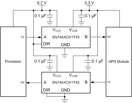
Figure 9-3 shows the SN74AXCH1T45 being used for the two-bit UART interface application. One SN74AXCH1T45 device is used to level shift the voltage and drive the TX from the processor to the GPS Module while a second SN74AXCH1T45 device is used to drive the TX Data line from the GPS Module to the Processor. Devices with bus-hold inputs remove the requirement for external pullup resistors to maintain a valid logic level at the input.
 Figure 9-3 UART Interface Application