SCDS136C October 2003 – May 2018 SN74CB3T3245
PRODUCTION DATA.
- 1 Features
- 2 Applications
- 3 Description
- 4 Revision History
- 5 Pin Configuration and Functions
- 6 Specifications
- 7 Parameter Measurement Information
- 8 Detailed Description
- 9 Application and Implementation
- 10Power Supply Recommendations
- 11Layout
- 12Device and Documentation Support
- 13Mechanical, Packaging, and Orderable Information
Package Options
Refer to the PDF data sheet for device specific package drawings
Mechanical Data (Package|Pins)
- DGV|20
- DBQ|20
- DW|20
- PW|20
Thermal pad, mechanical data (Package|Pins)
- PW|20
Orderable Information
8.2 Functional Block Diagram

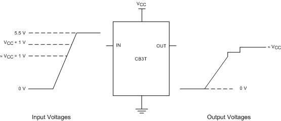
If the input high voltage (VIH) level is greater than or equal to VCC + 1V, and less than or equal to 5.5V, the output high voltage (VOH) level will be equal to approximately the VCC voltage level.
Figure 5. Typical DC Voltage Translation Characteristics
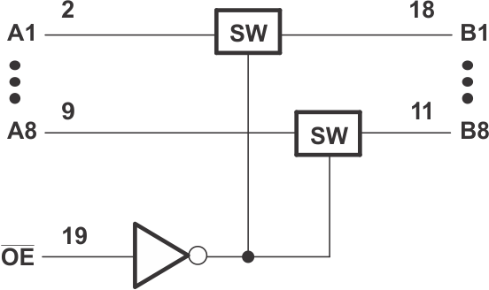
 Figure 6. Logic Diagram (Positive Logic)
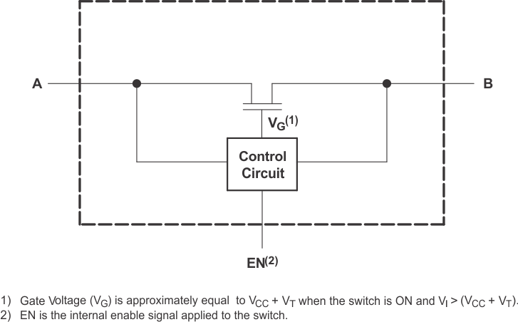
 Figure 7. Simplified Schematic, Each FET Switch (SW)