SCDS305D February 2011 – September 2022 SN74GTL2003
PRODUCTION DATA
- 1 Features
- 2 Applications
- 3 Description
- 4 Revision History
- 5 Pin Configuration and Functions
- 6 Specifications
- 7 Parameter Measurement Information
- 8 Detailed Description
- 9 Application and Implementation
- 10Power Supply Recommendations
- 11Layout
- 12Device and Documentation Support
- 13Mechanical, Packaging, and Orderable Information
Package Options
Mechanical Data (Package|Pins)
Thermal pad, mechanical data (Package|Pins)
Orderable Information
9.2.2.2.1 Sizing Pullup Resistors
The pullup resistor value should limit the current through the pass transistor when it is in the on state to about 15 mA. This ensures a pass voltage of 260 mV to 350 mV. If the current through the pass transistor is higher than 15 mA, the pass voltage also is higher in the on state. To set the current through each pass transistor at 15 mA, the pullup resistor value is calculated as:
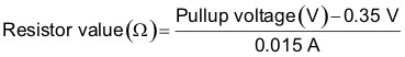
Table 9-2 provides resistor values for various reference voltages and currents at 15 mA, 10 mA, and 3 mA. The resistor value shown in the +10% column, or a larger value, should be used to ensure that the pass voltage of the transistor would be 350 mV or less. The external driver must be able to sink the total current from the resistors on both sides of the GTL device at 0.175 V, although the 15 mA only applies to current flowing through the SN74GTL2003.
| PULLUP RESISTOR VALUE (Ω) | ||||||
|---|---|---|---|---|---|---|
| VOLTAGE | 15 mA | 10 mA | 3 mA | |||
| NOMINAL | +10% | NOMINAL | +10% | NOMINAL | +10% | |
| 5.0 V | 310 | 341 | 465 | 512 | 1550 | 1705 |
| 3.3 V | 197 | 217 | 295 | 325 | 983 | 1082 |
| 2.5 V | 143 | 158 | 215 | 237 | 717 | 788 |
| 1.8 V | 97 | 106 | 145 | 160 | 483 | 532 |
| 1.5 V | 77 | 85 | 115 | 127 | 383 | 422 |
| 1.2 V | 57 | 63 | 85 | 94 | 283 | 312 |