SCDS305D February 2011 – September 2022 SN74GTL2003
PRODUCTION DATA
- 1 Features
- 2 Applications
- 3 Description
- 4 Revision History
- 5 Pin Configuration and Functions
- 6 Specifications
- 7 Parameter Measurement Information
- 8 Detailed Description
- 9 Application and Implementation
- 10Power Supply Recommendations
- 11Layout
- 12Device and Documentation Support
- 13Mechanical, Packaging, and Orderable Information
Package Options
Mechanical Data (Package|Pins)
Thermal pad, mechanical data (Package|Pins)
Orderable Information
3 Description
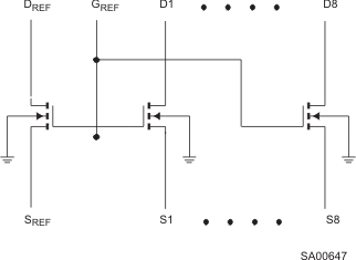
The SN74GTL2003 device provides eight NMOS pass transistors (Sn and Dn) with a common gate (GREF) and a reference transistor (SREF and DREF). The low ON-state resistance of the switch allows connections to be made with minimal propagation delay. With no direction control pin required, the device allows bidirectional voltage translations any voltage (0.95 V to 5 V) to any voltage (0.95 V to 5 V).
All transistors in the SN74GTL2003 have the same electrical characteristics, and there is minimal deviation from one output to another in voltage or propagation delay. This offers superior matching over discrete transistor voltage-translation solutions where the fabrication of the transistors is not symmetrical. With all transistors being identical, the reference transistor (SREF/DREF) can be located on any of the other eight matched Sn/Dn transistors, allowing for easier board layout. The translator transistors with integrated ESD circuitry provides excellent ESD protection.
| PART NUMBER | PACKAGE | BODY SIZE (NOM) |
|---|---|---|
| SN74GTL2003 | PW (TSSOP, 20) | 6.50 mm × 4.40 mm |
| RKS (VQFN, 20) | 4.50 mm × 2.50 mm |
 Simplified Clamp Schematic