SCDS305D February   2011  – September 2022 SN74GTL2003

PRODUCTION DATA  

  1. Features
  2. Applications
  3. Description
  4. Revision History
  5. Pin Configuration and Functions
  6. Specifications
    1. 6.1 Absolute Maximum Ratings
    2. 6.2 ESD Ratings
    3. 6.3 Recommended Operating Conditions
    4. 6.4 Thermal Information
    5. 6.5 Electrical Characteristics
    6. 6.6 Switching Characteristics
    7. 6.7 Switching Characteristics
    8. 6.8 Typical Characteristics
  7. Parameter Measurement Information
  8. Detailed Description
    1. 8.1 Overview
    2. 8.2 Functional Block Diagram
    3. 8.3 Feature Description
      1. 8.3.1 Provides Bidirectional Voltage Translation With No Direction Control Required
      2. 8.3.2 Flow Through Pinout
    4. 8.4 Device Functional Modes
  9. Application and Implementation
    1. 9.1 Application Information
    2. 9.2 Typical Applications
      1. 9.2.1 Bidirectional Translation
        1. 9.2.1.1 Design Requirements
        2. 9.2.1.2 Detailed Design Procedure
          1. 9.2.1.2.1 Sizing Pullup Resistors
        3. 9.2.1.3 Application Curve
      2. 9.2.2 Unidirectional Down Translation
        1. 9.2.2.1 Design Requirements
        2. 9.2.2.2 Detailed Design Procedure
          1. 9.2.2.2.1 Sizing Pullup Resistors
      3. 9.2.3 Unidirectional Up Translation
        1. 9.2.3.1 Design Requirements
        2. 9.2.3.2 Detailed Design Procedure
          1. 9.2.3.2.1 Sizing Pullup Resistors
  10. 10Power Supply Recommendations
  11. 11Layout
    1. 11.1 Layout Guidelines
    2. 11.2 Layout Example
  12. 12Device and Documentation Support
    1. 12.1 Receiving Notification of Documentation Updates
    2. 12.2 Receiving Notification of Documentation Updates
    3. 12.3 Support Resources
    4. 12.4 Trademarks
    5. 12.5 Electrostatic Discharge Caution
    6. 12.6 Glossary
  13. 13Mechanical, Packaging, and Orderable Information

Package Options

Mechanical Data (Package|Pins)
Thermal pad, mechanical data (Package|Pins)
Orderable Information

Unidirectional Down Translation

For unidirectional clamping (higher voltage to lower voltage), the GREF input must be connected to DREF and both pins pulled to the higher-side VCC through a pullup resistor (typically 200 kΩ). TI recommends a filter capacitor on DREF. Pullup resistors are required if the chipset I/Os are open drain. The opposite side of the reference transistor (SREF) is connected to the processor core power supply voltage. When DREF is connected through a 200-kΩ resistor to a 3.3-V to 5.5-V VCC supply and SREF is set from 1 V to VCC – 1.5 V, the output of each Sn has a maximum output voltage equal to SREF.
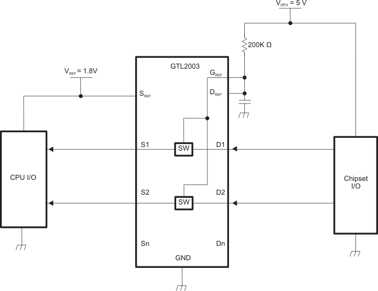
GUID-9FABA3D9-3EC2-4A37-8653-606433F8A29C-low.gif Figure 9-3 Unidirectional Down Translation to Protect Low-Voltage Processor Pins