SCDS305D February   2011  – September 2022 SN74GTL2003

PRODUCTION DATA  

  1. Features
  2. Applications
  3. Description
  4. Revision History
  5. Pin Configuration and Functions
  6. Specifications
    1. 6.1 Absolute Maximum Ratings
    2. 6.2 ESD Ratings
    3. 6.3 Recommended Operating Conditions
    4. 6.4 Thermal Information
    5. 6.5 Electrical Characteristics
    6. 6.6 Switching Characteristics
    7. 6.7 Switching Characteristics
    8. 6.8 Typical Characteristics
  7. Parameter Measurement Information
  8. Detailed Description
    1. 8.1 Overview
    2. 8.2 Functional Block Diagram
    3. 8.3 Feature Description
      1. 8.3.1 Provides Bidirectional Voltage Translation With No Direction Control Required
      2. 8.3.2 Flow Through Pinout
    4. 8.4 Device Functional Modes
  9. Application and Implementation
    1. 9.1 Application Information
    2. 9.2 Typical Applications
      1. 9.2.1 Bidirectional Translation
        1. 9.2.1.1 Design Requirements
        2. 9.2.1.2 Detailed Design Procedure
          1. 9.2.1.2.1 Sizing Pullup Resistors
        3. 9.2.1.3 Application Curve
      2. 9.2.2 Unidirectional Down Translation
        1. 9.2.2.1 Design Requirements
        2. 9.2.2.2 Detailed Design Procedure
          1. 9.2.2.2.1 Sizing Pullup Resistors
      3. 9.2.3 Unidirectional Up Translation
        1. 9.2.3.1 Design Requirements
        2. 9.2.3.2 Detailed Design Procedure
          1. 9.2.3.2.1 Sizing Pullup Resistors
  10. 10Power Supply Recommendations
  11. 11Layout
    1. 11.1 Layout Guidelines
    2. 11.2 Layout Example
  12. 12Device and Documentation Support
    1. 12.1 Receiving Notification of Documentation Updates
    2. 12.2 Receiving Notification of Documentation Updates
    3. 12.3 Support Resources
    4. 12.4 Trademarks
    5. 12.5 Electrostatic Discharge Caution
    6. 12.6 Glossary
  13. 13Mechanical, Packaging, and Orderable Information

Package Options

Mechanical Data (Package|Pins)
Thermal pad, mechanical data (Package|Pins)
Orderable Information

Parameter Measurement Information

CL = Load Capacitance, includes jig and probe capacitance (see Section 6.5 for value)
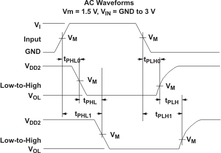
GUID-F6EC84AB-2956-43A8-A492-025694455533-low.gifFigure 7-1 Input (Sn) to Output (Dn) Propagation Delays
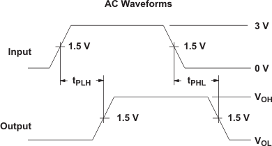
GUID-988CEEC8-7B28-4D8D-8922-D1C3CE1A6C18-low.gifFigure 7-3 Input (Sn) to Output (Dn) Propagation Delays
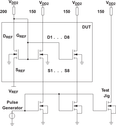
GUID-5EEB6214-0827-4F93-BFAF-ED4DDBEAF87E-low.gifFigure 7-2 Load Circuit
GUID-03BF06BB-DE9F-447A-83D8-FDC04385C7B7-low.gifFigure 7-4 Load Circuit
Table 7-1 Test Conditions
TEST S1
tpd Open
tPLZ/tPZL 7 V
TPHZ/TPZH Open