SCLS402R April 1998 – March 2023 SN74LV165A
PRODMIX
- 1 Features
- 2 Applications
- 3 Description
- 4 Revision History
- 5 Pin Configuration and Functions
-
6 Specifications
- 6.1 Absolute Maximum Ratings
- 6.2 ESD Ratings
- 6.3 Recommended Operating Conditions
- 6.4 Thermal Information
- 6.5 Electrical Characteristics
- 6.6 Timing Requirements, VCC = 2.5 V ± 0.2 V
- 6.7 Timing Requirements, VCC = 3.3 V ± 0.3 V
- 6.8 Timing Requirements, VCC = 5 V ± 0.5 V
- 6.9 Switching Characteristics, VCC = 2.5 V ± 0.2 V
- 6.10 Switching Characteristics, VCC = 3.3 V ± 0.3 V
- 6.11 Switching Characteristics,VCC = 5 V ± 0.5 V
- 6.12 Timing Diagrams
- 6.13 Operating Characteristics
- 6.14 Typical Characteristics
- 7 Parameter Measurement Information
- 8 Detailed Description
- 9 Application and Implementation
- 10Device and Documentation Support
- 11Mechanical, Packaging, and Orderable Information
3 Description
The SN74LV165A device is a parallel-load, 8-bit shift registers designed for 2 V to 5.5 V VCC operation.
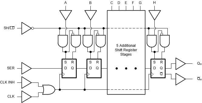
When the device is clocked, data is shifted toward the serial output QH. Parallel-in access to each stage is provided by eight individual direct data inputs that are enabled by a low level at the shift/load (SH/ LD) input. The 'LV165A devices feature a clock-inhibit function and a complemented serial output, QH.
This device is fully specified for partial-power-down applications using Ioff. The Ioff circuitry disables the outputs, preventing damaging current backflow through the devices when they are powered down.
| PART NUMBER | PACKAGE | BODY SIZE (NOM) |
|---|---|---|
| SN74LV165A | D (SOIC, 16) | 9.90 mm × 3.90 mm |
| DB (SSOP, 16) | 6.20 mm × 5.30 mm | |
| NS (SO, 16) | 10.20 mm × 5.30 mm | |
| PW (TSSOP, 16) | 5.00 mm × 4.40 mm | |
| DGV (TVSOP, 16) | 3.60 mm × 4.40 mm | |
| RGY (VQFN, 16) | 4.00 mm × 3.50 mm | |
| BQB (WQFN, 16) | 3.60 mm × 2.60 mm |
 Logic Diagram (Positive Logic)