SCAS291W MARCH 1993 – October 2016 SN54LVC138A , SN74LVC138A
PRODUCTION DATA.
- 1 Features
- 2 Applications
- 3 Description
- 4 Revision History
- 5 Pin Configuration and Functions
- 6 Specifications
- 7 Parameter Measurement Information
- 8 Detailed Description
- 9 Application and Implementation
- 10Power Supply Recommendations
- 11Layout
- 12Device and Documentation Support
- 13Mechanical, Packaging, and Orderable Information
Package Options
Refer to the PDF data sheet for device specific package drawings
Mechanical Data (Package|Pins)
- DB|16
- PW|16
- NS|16
- RGY|16
- D|16
- DGV|16
- RSV|16
Thermal pad, mechanical data (Package|Pins)
- RGY|16
Orderable Information
1 Features
2 Applications
- LED Displays
- Servers
- White Goods
- Power Infrastructure
- Building Automation
- Factory Automation
3 Description
The SN74LVC138A devices are designed for high-performance memory-decoding or data-routing applications requiring very short propagation delay times. In high-performance memory systems, these decoders minimize the effects of system decoding. When employed with high-speed memories using a fast enable circuit, delay times of these decoders and the enable time of the memory usually are less than the typical access time of the memory. This means that the effective system delay introduced by the decoders is negligible.
Device Information(1)
| PART NUMBER | PACKAGE | BODY SIZE (NOM) |
|---|---|---|
| SNx4LVC138A | LCCC (20) | 8.89 mm × 8.89 mm |
| CDIP (16) | 19.56 mm × 6.92 mm | |
| CFP (16) | 10.30 mm × 6.73 mm | |
| SOIC (16) | 9.90 mm × 3.91 mm | |
| SSOP (16) | 6.20 mm × 5.30 mm | |
| TVSOP (16) | 3.60 mm × 4.40 mm | |
| BGA MICROSTAR JUNIOR (20) | 4.00 mm × 3.00 mm | |
| TSSOP (16) | 5.00 mm × 4.40 mm | |
| UQFN (16) | 2.60 mm × 1.80 mm |
- For all available packages, see the orderable addendum at the end of the data sheet.
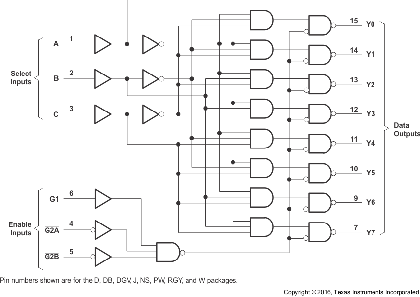
Logic Diagram (Positive Logic)
