SCES586D July 2004 – June 2015 SN74LVC1G123
PRODUCTION DATA.
- 1 Features
- 2 Applications
- 3 Description
- 4 Revision History
- 5 Pin Configuration and Functions
-
6 Specifications
- 6.1 Absolute Maximum Ratings
- 6.2 ESD Ratings
- 6.3 Recommended Operating Conditions
- 6.4 Thermal Information
- 6.5 Electrical Characteristics
- 6.6 Timing Requirements
- 6.7 Switching Characteristics, CL = 15 pF, -40°C to 85°C
- 6.8 Switching Characteristics, CL = 50 pF, -40°C to 85°C
- 6.9 Switching Characteristics, CL = 50 pF, -40°C to 125°C
- 6.10 Operating Characteristics
- 6.11 Typical Characteristics
- 7 Parameter Measurement Information
- 8 Detailed Description
- 9 Application and Implementation
- 10Power Supply Recommendations
- 11Layout
- 12Device and Documentation Support
- 13Mechanical, Packaging, and Orderable Information
Package Options
Mechanical Data (Package|Pins)
Thermal pad, mechanical data (Package|Pins)
Orderable Information
9 Application and Implementation
NOTE
Information in the following applications sections is not part of the TI component specification, and TI does not warrant its accuracy or completeness. TI’s customers are responsible for determining suitability of components for their purposes. Customers should validate and test their design implementation to confirm system functionality.
9.1 Application Information
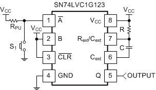
The SN74LVC1G123 can be used for many applications. The application shown here is a switch debounce circuit. Many switches produce multiple triggers when pressed, and the debounce circuit turns the many triggers into one. This circuit takes advantage of the retrigger capability of the SN74LVC1G123 in that the output pulse length only has to be longer than the longest individual bounce (typically less than 1 ms).
9.2 Typical Application
 Figure 10. Typical Application of the SN74LVC1G123
9.2.1 Design Requirements
- Recommended Input Conditions:
- For specified high and low levels, see VIH and VIL in Recommended Operating Conditions.
- Inputs and outputs are overvoltage tolerant, allowing them to go as high as 4.6 V at any valid VCC.
- Recommended Output Conditions:
- Load current should not exceed values listed in Recommended Operating Conditions.
9.2.2 Detailed Design Procedure
The values for VCC, RPU, R, and C must be selected for proper operation.
VCC is selected at 1.8 V. This value is usually driven by the logic voltage of the system, but is arbitrary in this case.
RPU is selected at 10 kΩ.
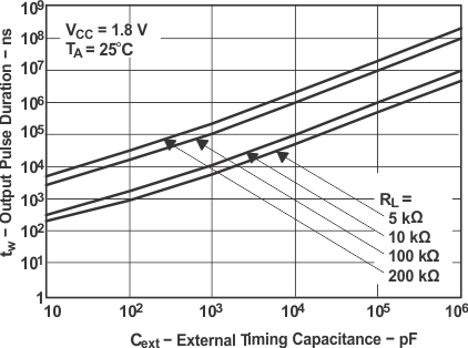
R and C are selected via the plots in Application Curves and are based on the time desired for the output pulse. In this case, the output pulse will be 1 ms. Since the supply voltage has been selected at 1.8 V, Figure 11 is used to determine the R and C values required. First convert the desired pulse width (tw), 1 ms, to ns. This yields 106 ns. Next follow that line across to see which R and C values intersect it.
R is selected at 10 kΩ because that line intersects nicely with 106 ns and 105 pF, making the selection of C at 0.1 µF easy.
Table 2. Application Specific Values
| PARAMETER | VALUE |
|---|---|
| VCC | 1.8 V |
| RPU | 10 kΩ |
| tw | 1 ms |
| R (Rext) | 10 kΩ |
| C (Cext) | 0.1 µF |
In addition to the shown components, a 0.1-µF decoupling capacitor from VCC to ground should be placed as close as possible to the device.
9.2.3 Application Curves
 Figure 11. Output Pulse Duration
 vs External Timing Capacitance
 Figure 13. Output Pulse Duration
 vs External Timing Capacitance
 Figure 15. Minimum Retrigger Time
 vs Supply Voltage
 Figure 12. Output Pulse Duration
 vs External Timing Capacitance
 Figure 14. Output Pulse Duration Constant
 vs Supply Voltage